Attention
This document was last updated Dec 07 24 at 10:12
Project: A hardware-accelerated MAC function
This course includes a design project that follows the ASIC design flow we studied. You will complete the project in your designated/chosen team. To find out which team you belong to, go to Canvas, and check under ‘People’ and then ‘Team’. Every team member will share the same grade for the project. Team Size will not influence the grade that a project can attain.
The project target is to build a hardware acceleration of a reference implementation of Poly1305, described in IETF RFC 7539. This algorithm implements a Message Authentication Code. Given a message, such as Cryptographic Forum Research Group, and a 128-bit secret key, such as 85:d6:be:78:57:55:6d:33:7f:44:52:fe:42:d5:06:a8:01:03:80:8a:fb:0d:b2:fd:4a:bf:f6:af:41:49:f5:1b, Poly1305 computes a 64-bit tag. For the example given the tag is a8:06:1d:c1:30:51:36:c6:c2:2b:8b:af:0c:01:27:a9. The tag authenticates the message, which means that the tag demonstrates that it must be produced by someone who knows the message and the secret key. MAC codes are used in a wide variety of internet security applications, but also for example in electronic door lock applications. A door lock emits a challenge (a random message), and the wireless key responds with the MAC of the message. If both the door lock and the key are programmed with a matching secret key, the door lock can now verify if the received tag matches the tag that it computes locally.
The project’s objective will be for you to implement a hardware version of the Poly1305 algorithm that can be integrated in an SoC. Your starting point will be a reference implementation of an SoC that implements the Poly1305 algorithm in hardware. Hence, the focus of the design will be on thinking about hardware strategies to map (and accelerate) Poly1305 as a coprocessor.
The project spans four phases. In each phase, you have to prepare a small report or presentation and meet 1-1 with the instructor. Each phase will be graded separately, with the final phase culminating in a class presentation of your work. As there are a large number of teams (12), your time to report your results in 1-1 sessions is limited. Please come prepared!
Project Timeline
The project runs over 5 weeks (including Thanksgiving week).
Week |
Topic |
Deliverable |
Location |
|---|---|---|---|
13 November |
Project Definition |
Team Meeting Presentation |
AK 301 or Video |
20 November |
Project Design |
Team Meeting Presentation |
AK 301 or Video |
4 December |
Project Implementation |
Team Meeting Presentation |
AK 301 or Video |
11 December |
Project Presentation |
Class Presentation |
AK 232 or Video |
Project meetings will be between team members and the instructor in AK 301 during the initial stages of the project. Project meetings allocate 15 minutes per team. The project members prepare for the meeting by means a a short presentation to explain their plans and/or progress. The instructor will ask for clarification or enhancements where needed. The team members will have a chance to explain and motivate their plans.
For students in the synchronous version of the course, the meetings will be scheduled in AK 301 during class time on Wednesdays. The meeting schedule will be posted on Canvas, and students will be able to sign up for a slot according to their preference.
Students in the asynchronous version of the course must prepare a video presentation and share it with the instructor. Students will receive feedback by email. Alternately, online students may sign up for a synchronous zoom slot during class time on Wednesdays. In the latter case, the meeting schedule will be posted on Canvas, and students will be able to sign up for a slot according to their preference.
The final lecture will consist of an in-class presentation by each team in the synchronous version of the course. Project presentations must include a formal presentation with slides, and will be made in a conference style format with moderated Q&A. Students in the asynchronous version of the course must prepare a video presentation, but will have a chance to present their work in the final synchronous lecture as well.
Reference Implementation
Attention
To understand the following, it may be useful to revisit the System On Chip lecture. To start, you will need to accept the final assignment to receive the reference implementation at the following Github Classroom link. This will give you a repository final-project-userid which you can clone to the class server.
The reference implementation is an IBEX based SoC with a 32-bit RISCV core, 2MB of RAM, a UART, a timer, a GPIO port, and SPI. The following are key design files that you should study:
custom/rtl/top_rtl.svChip top-level of the SoC. The SoC only uses clock, reset, a GPIO input and a GPIO output port.custom/rtl/custom_ibex.svSoC system architecture that instantiates the IBEX, a bus, and various peripherals.custom/rtl/myreg.svExample of a custom user-defined peripheral, in this case a collection of two registers which can be read from/ written to from software running on IBEX.Makefileto drive the design process: compiling software, the simulation, the hardware, and so on.sw/c/demo/poly1305Reference software implementation of the Poly1305 algorithm.
This initial repository will emphasize RTL design and simulation using Verilator. In later stages of the project, we will introduce a hardware synthesis flow to map the hardware to a standard cell netlist. The following steps demonstrate a basic walkthrough of the reference design.
Environment setup
You will need fusesoc and Verilator so make sure you setup the environment correctly with
pyenv activate fusesoc
scl enable devtoolset-9 bash
If needed revisit the notes of System On Chip
Inspecting and Compiling software
Let’s start with the Poly1305 software implementation. This lab assignment does not explain you how poly1305 works. Instead, refer to IETF RFC 7539. Writing cryptographic algorithms involves many bits, and it’s important that you understand the notations used, such as octet string, number and message. All these conventions are explained clearly in the RFC.
First, inspect the files in sw/c/demo/poly1305.
poly1305.{c,h}contains the reference implementation in software.main.cis the main driver program that computes the tag for a reference message, while measuring clock cyclesrfc7539.txtis FYI, the text of the RFC.polygen.cis a test program to compute MACs for test messages. This program will not run on the IBEX, you can simply compile with with gcc. It will not be further discussed below.
Now, let’s take a look at the main function in main.c. A MAC is a
function that can, in principle, process arbitrary-length
messages. Hence, for a given key, Poly1305 can compute a tag no matter
how long or how short the message really is. The software
implementation gets around this flexibility requirement by
partitioning the MAC computation in phases. Typically, there is an
initialization phase that sets up the internal MAC state, followed by
one or more update phases that feed in a block of message bytes while
updating the MAC state, and a terminating phase that extracts the tag
from the MAC state. This implemenentation of Poly1305 is no different, and
you can spot poly1305Init, poly1305Update and poly1305Final.
Besides the MAC processing, you can also spot the use of the timer, which is called just before and after calling a Poly1305 phase. That will give us an idea of the implementation cost (execution time).
 void main() {

  Poly1305Context c;

  uint64_t init_cycles;
  uint64_t block_cycles;
  uint64_t final_cycles;
  uint64_t stamp;

  timer_init();

  puts("--key:\n");
  stamp = timer_read();
  poly1305Init(&c, key);
  init_cycles = timer_read() - stamp;
  showPoly(&c);

  puts("--block1:\n");
  stamp = timer_read();
  poly1305Update(&c, block1, block1len);
  block_cycles = timer_read() - stamp;
  showPoly(&c);

  puts("--block2:\n");
  poly1305Update(&c, block2, block2len);
  showPoly(&c);

  puts("--block3:\n");
  poly1305Update(&c, block3, block3len);
  showPoly(&c);

  puts("--final:\n");
  stamp = timer_read();
  poly1305Final(&c, tag);
  final_cycles = timer_read() - stamp;
  showPoly(&c);

  puts("--tag:\n");
  showBlock(tag, 16);

  puts("--poly1305 performance:\n");
  puts("Init:  ");
  puthex((uint32_t) (init_cycles >> 32));
  puthex((uint32_t) (init_cycles));
  putchar('\n');
  puts("Block: ");
  puthex((uint32_t) (block_cycles >> 32));
  puthex((uint32_t) (block_cycles));
  putchar('\n');
  puts("Final: ");
  puthex((uint32_t) (final_cycles >> 32));
  puthex((uint32_t) (final_cycles));
  putchar('\n');

  // delay the simulator before halting so all output is flushed
  stamp = timer_read();
  while ((timer_read() - stamp) < 700000) ;

  sim_halt();
}
To compile the software, use the following command from the main entry point of your final project repo.
make swprep
If you make a change to the software and you want to force recompilation, use the -B command line parameter:
make -B swprep
Inspecting and Compiling hardware
The reference hardware is based on the Custom IBEX example discussed in Lecture 2.
The toplevel of the design is defined in custom/rtl/top_rtl.sv, and the SOC itself
is defined in custom/rtl/custom_ibex.sv.
The following steps show you how to construct the simulator for this system.
The resulting simulation is put in build/custom_ibex_0/sim-verilator/
make simprep
Running the simulation
When we run the simulation, we will load a compiled binary of an IBEX firmware
application into the RAM, and then execute the Verilator executable.
This simulation also simulates the UART which is used for various output operations
(putchar and puts in the C program). So, you will not see the UART output
appear on screen. Instead, the output is dumped in a file called uart0.log.
The easiest is to open a second terminal, and monitor this file as follows. The -f flag on tail ensures that any new updates to the file will be displayed on the console of the second terminal.
tail -f uart0.log
In the original (first) terminal, you can now run the simulation with:
make run
In the second terminal, you will note the following output:
tail: uart0.log: file truncated
--key:
R  as a number 0806D540 0E52447C 036D5554 08BED685
S  as a number 1BF54941 AFF6BF4A FDB20DFB 8A800301
A* as a number 00000000 00000000 00000000 00000000 00000000
Buffer 0000000000000000000000000000000000 ()
--block1:
R  as a number 0806D540 0E52447C 036D5554 08BED685
S  as a number 1BF54941 AFF6BF4A FDB20DFB 8A800301
A* as a number 00000002 C88C7784 9D64AE91 47DDEB88 E69C83FC
Buffer 43727970746F6772617068696320466F01 (Cryptographic Fo)
--block2:
R  as a number 0806D540 0E52447C 036D5554 08BED685
S  as a number 1BF54941 AFF6BF4A FDB20DFB 8A800301
A* as a number 00000002 D8ADAF23 B0337FA7 CCCFB4EA 344B30DE
Buffer 72756D2052657365617263682047726F01 (rum Research Gro)
--block3:
R  as a number 0806D540 0E52447C 036D5554 08BED685
S  as a number 1BF54941 AFF6BF4A FDB20DFB 8A800301
A* as a number 00000002 D8ADAF23 B0337FA7 CCCFB4EA 344B30DE
Buffer 75706D2052657365617263682047726F01 (upm Research Gro)
--final:
R  as a number 00000000 00000000 00000000 00000000
S  as a number 00000000 00000000 00000000 00000000
A* as a number 00000000 00000000 00000000 00000000 00000000
Buffer 7570010000000000000000000000000000 (up)
--tag:
A8061DC1305136C6C22B8BAF0C0127A9
--poly1305 performance:
Init:  00000000000001BB
Block: 0000000000000D3A
Final: 000000000000111A
While in the first terminal, you will see:
[pschaumont@arc-schaumont-class-vm final-project-patrickschaumont]$ make run
Simulation of Custom Ibex System
==============================

Tracing can be toggled by sending SIGUSR1 to this process:
$ kill -USR1 17838

UART: Created /dev/pts/9 for uart0. Connect to it with any terminal program, e.g.
$ screen /dev/pts/9
UART: Additionally writing all UART output to 'uart0.log'.

Simulation running, end by pressing CTRL-c.
Terminating simulation by software request.
- ../src/lowrisc_ibex_sim_shared_0/./rtl/sim/simulator_ctrl.sv:93: Verilog $finish
Received $finish() from Verilog, shutting down simulation.

Simulation statistics
=====================
Executed cycles:  5926399
Wallclock time:   12.932 s
Simulation speed: 458274 cycles/s (458.274 kHz)

Performance Counters
====================
Cycles:                     5926395
Instructions Retired:       3135341
LSU Busy:                   1208436
Fetch Wait:                 1035040
Loads:                      1146947
Stores:                     61489
Jumps:                      34858
Conditional Branches:       552483
Taken Conditional Branches: 512180
Take a moment to observe this data. The output of the C simulation should match the example of Poly1305 in the RFC standard. In the main simulation window, you notice various performance metrics. Note the very high simulation speed (>400KHz) thanks to cycle-accurate compiled simulation without any VCD/FST tracing.
There is an alternate version of the run command called runfst which creates a signal
trace file of all signals in the simulation. This will obviously slow down the simulation
significantly (to 40KHz, so 10x slower). Also the fst file is very large (280MB).
make runfst
The fst file can be opened with gtkwave. Once we will design custom hardware for Poly1305, this waveform feature will become a useful extension.
Project Definition Phase
Your assignment for this week in the final project is as follows.
Set up the final project design environment as outlined above.
Study the Poly1305 algorithm, in particular by carefully reading the RFC document (Section 2.5)
Do research on the fundamental operation performed by Poly1305: (r * a) % p. In particular, p is a prime number with a special form: 2^130 - 5. Find out how this leads to an efficient implementation in hardware and software.
Make a short presentation (5 slides max) on your findings. As the final slide, present your ideas on how to accelerate Poly1305 in hardware.
Project Design Phase
Your assignment for this week in the final project is as follows.
Make a detailed block diagram of a Poly1305 hardware accelerator. Your block diagram should show every register used in your hardware accelerator, as well as individual blocks for datapath logic. Your block diagram should enumerate all I/O ports used at the top-level. Finite state machines (with embedded state register) may be drawn as boxes as well. Your block diagram must reflect a potential RTL design with as much detail as needed, such that the RTL coding becomes easy.
Describe the hardware/software interface between IBEX and your hardware accelerator in detail. For example, in the myreg.sv example hardware module (found in your final project github under
custom/rtl/myreg.sv), two registers are defined:reg1andreg2. For each such memory-mapped register in your hardware/software interface, define its length, direction (sw to hw, or hw to sw, or bidrectional), and functionality. Provide pseudocode that shows how your C application on the IBEX will communicate with your hardware accelerator.
Make a short presentation (5 slides max) with your design. As the final slide, make a back-of-the-envelope calculation that shows how much faster your hardware design will be over a pure software implementation.
The following slides (PDF) capture
the main idea of Poly1305 hardware implementation. However, while
the Verilog code as shown is correct, it is inefficient for
hardware implementation because of the massive hardware
multiplier. Your task is to come up with a hardware implementation
strategy that is much more compact than this design, while still
ensuring reasonable hardware acceleration performance.
Attention
A few groups asked about the full testbench shown in the slides. The complete testbench
is listed below. You can use polygen.c and poly1305.c to generate additional
testvectors that can be read by this testbench.
module tb;
 reg [127:0]  r;
 reg [127:0]  s;
 reg [127:0]  m;
 reg          fb;
 reg          ld;
 reg          first;
 wire [127:0] p;
 wire         rdy;
 reg          reset;
 reg          clk;

 poly1305 dut(.reset(reset),
              .clk(clk),
              .r(r),
              .s(s),
              .m(m),
              .fb(fb),
              .ld(ld),
              .first(first),
              .p(p),
              .rdy(rdy));

 always
   begin
      clk = 1'b0;
      #5;
      clk = 1'b1;
      #5;
   end

 reg [514:0] inputvector;
 integer     inputfile;

 reg         tv_firstblock;
 reg         tv_lastblock;
 reg         tv_fullblock;
 reg [127:0] tv_data;
 reg [255:0] tv_key;
 reg [127:0] tv_tag;
 reg [127:0] tv_tag_swap;

 integer     i;

 initial
   begin
      $dumpfile("trace.vcd");
      $dumpvars(0, tb);
      inputfile = $fopen("vectors.txt","r");

      r = 128'h0;
      s = 128'h0;
      m = 128'h0;
      fb = 1'b0; // fulblock
      ld = 1'b0;
      first = 1'b0;

      reset = 1'b1;
      repeat(3)
        @(posedge clk);

      reset = 1'b0;
      @(posedge clk);

      while (!$feof(inputfile))
        begin

           $fscanf(inputfile, "%b", inputvector);

           {tv_firstblock,
            tv_lastblock,
            tv_fullblock,
            tv_data,
            tv_key,
            tv_tag} = inputvector;

           r = 128'b0;
           s = 128'b0;
           for (i = 0; i < 16; i = i + 1)
             begin
                s = (s << 8) | tv_key[7:0];
                tv_key = (tv_key >> 8);
             end
           for (i = 0; i < 16; i = i + 1)
             begin
                r = (r << 8) | tv_key[7:0];
                tv_key = (tv_key >> 8);
             end

           m = 128'b0;
           for (i = 0; i < 16; i = i + 1)
             begin
                m = (m << 8) | tv_data[7:0];
                tv_data = (tv_data >> 8);
             end

           first = tv_firstblock;
           fb = tv_fullblock;

           ld = 1'b1;
           @(posedge clk);

           while (rdy == 1'b0)
             begin
                ld = 1'b0;
                @(posedge clk);
             end

           tv_tag_swap = 128'b0;
           for (i = 0; i < 16; i = i + 1)
             begin
                tv_tag_swap = (tv_tag_swap << 8) | tv_tag[7:0];
                tv_tag = (tv_tag >> 8);
             end

           if ((tv_lastblock == 1'b1) && (p != tv_tag_swap))
             $display("Expected tag %x but computed %x", tv_tag_swap, p);
           else if (tv_lastblock == 1'b1)
             $display("Tag OK: %x", p);
        end


      $finish;
   end

endmodule
 module processblock(input          reset,
                  input          clk,
                  input [127:0]  r,
                  input [128:0]  m, // {1, 128 message bits}
                  input [129:0]  a_in, // {acc < P = 2^130 - 5}
                  output [129:0] a_out,
                  input          start,
                  output         done
                  );

 wire [130:0]                    m1;
 wire [258:0]                    m2; // 128 bits * 131 bits = 259 bits
 wire [131:0]                    m3; // first reduction leaves 2 extra bits
 wire [129:0]                    m4;
 wire [2:0]                      five;

 assign five = 5;
 assign m1 = m + a_in;
 assign m2 = m1 * r;
 assign m3 = m2[129:0] + m2[258:130] * five;  // first reduction
 assign a_out = m3[129:0] + m3[131:130] * five;  // second reduction
 assign done = start;

endmodule
 module poly1305(input          reset,
              input          clk,
              input [127:0]  r,
              input [127:0]  s,
              input [127:0]  m,
              input          fb,
              input          ld,
              input          first,
              output [127:0] p,
              output         rdy);
 // fb   ld    first
 // x    x     1      marks the first block of a sequence of blocks
 // 1    1     0      m contains 128 bits of message (and does not include separator byte)
 // 0    1     0      m contains <128 bits of message (and includes separator byte)
 // 0    0     x      processing cycle

 reg [129:0]                 acc;
 wire [129:0]                acc_out;
 wire [129:0]                acc_in;
 wire                        block_start;
 wire                        block_done;

 wire [128:0]                msep;
 assign msep = fb ? {1'b1, m} : m;

 assign acc_in = first ? 130'b0 : acc;

 wire [127:0]                rclamp;

 assign rclamp = r & 128'h0FFF_FFFC_0FFF_FFFC_0FFF_FFFC_0FFF_FFFF;

 processblock single(.reset(reset),
                     .clk  (clk),
                     .r    (rclamp),
                     .m    (msep),
                     .a_in (acc_in),
                     .a_out(acc_out),
                     .start(block_start),
                     .done (block_done)
                     );

 always @(posedge clk)
   if (reset)
     acc <= 130'h0;
   else
     acc <= block_done ? acc_out : acc;

 assign block_start = ld;

 assign p = acc_out + s;
 assign rdy = block_done;

endmodule
Project Implementation Phase
The final phase of the project is the implementation into RTL. Your objective is to build a systemverilog implementation of Poly1305 that can be integrated as a (memory-mapped) coprocessor core for the IBEX core.
Attention
In the following, we provide guidelines on the implementation of the
poly1305 coprocessor. You are free to follow your own path.
However, you must deliver at least the following final results.
First, you must provide an SoC level testbench, part of
your final-project-.. repository.
Next, you must provide a netlist (and possibly layout) of the
coprocessor implemented by itself. This requires a separate repository,
as explained below. Do not work on synthesis/layout until you have
a completely correct and working simulation in final-project-...
Study how myreg works
Refer to the myreg demonstration coprocessor to see how
memory-mapped registers can be created. In the following, the most
important features of myreg.sv are reviewed.
First, the coprocessor needs to provide a standard bus interface. This bus interface will be identical for your Poly1305 coprocessor. It includes the following signals.
clk_i, the clock inputrst_ni, the negative-asserted reset inputdevice_req_i, the device request input, asserted at valid bus cyclesdevice_addr_i, the relative address input (i.e. starts at 0 for this module)device_we_i, the write control input, asserted during write cyclesdevice_be_i, the byte-assert input, one bit per byte of a worddevice_wdata_i, the write data input (32 bit)device_rvalid_o, the read assertion output, asserted whendevice_rdata_ovaliddevice_rdata_o, the read data output (32 bit)
module myreg #(
   parameter int unsigned AddrWidth = 32,
   parameter int unsigned RegAddr   = 8
 ) (
   input logic                 clk_i,
   input logic                 rst_ni,

   input logic                 device_req_i,
   input logic [AddrWidth-1:0] device_addr_i,
   input logic                 device_we_i,
   input logic [3:0]           device_be_i,
   input logic [31:0]          device_wdata_i,
   output logic                device_rvalid_o,
   output logic [31:0]         device_rdata_o
 );
In a coprocessor, you would first create a read and write strobe for each memory mapped register. For each such register, you also choose a relative memory address, starting at 0. It’s a good practice to make memory-mapped registers both readable and writable from software. Even if you would use that register only to transfer data from software to hardware, it’s still useful for debugging if your system software can access that register.
localparam int              unsigned MYREG_REG1 = 32'h0;
localparam int              unsigned MYREG_REG2 = 32'h4;

logic [RegAddr-1:0]         reg_addr;
logic                       reg1_wr, reg1_rd, reg1_rd_d;
logic                       reg2_wr, reg2_rd, reg2_rd_d;

logic [31:0]                reg1_data;
logic [31:0]                reg2_data;


// Decode write and read requests.
assign reg_addr          = device_addr_i[RegAddr-1:0];
assign reg1_wr           = device_req_i &  device_we_i & (reg_addr == MYREG_REG1[RegAddr-1:0]);
assign reg1_rd           = device_req_i & ~device_we_i & (reg_addr == MYREG_REG1[RegAddr-1:0]);
assign reg2_wr           = device_req_i &  device_we_i & (reg_addr == MYREG_REG2[RegAddr-1:0]);
assign reg2_rd           = device_req_i & ~device_we_i & (reg_addr == MYREG_REG2[RegAddr-1:0]);
Next, you have to develop two pieces of logic, that show (a) how to
write into the memory mapped registers, and (b) how to read from the
memory mapped registers. The challenge of writing into the
memory-mapped registers, is that the software-based access must be
combined with the access coming from the custom hardware. In this case,
the myreg example shows something straightforward: if you write
into reg1, then reg2 will be updated at the same time with the
sum of (the previous) reg1 and reg2. Conversely, if you write into
reg2, then reg1 will be updated at the same time with the
sum of (the previous) reg1 and reg2. This results in the following code.
In the following code, also pay special attention to the creation of delayed
write strobes reg1_rd_d and reg2_rd_d. These are needed to support reading
from the memory mapped registers from software.
   always @(posedge clk_i or negedge rst_ni) begin
    if (!rst_ni) begin
     reg1_data <= 32'b0;
     reg2_data <= 32'b0;
     reg1_rd_d <= 1'b0;
     reg2_rd_d <= 1'b0;
    end else begin
     if (reg1_wr)
       begin
          reg1_data[7:0]   <= {device_be_i[0] ? device_wdata_i[7:0] : reg1_data[7:0]};
          reg1_data[15:8]  <= {device_be_i[1] ? device_wdata_i[15:8] : reg1_data[15:8]};
          reg1_data[23:16] <= {device_be_i[2] ? device_wdata_i[23:16] : reg1_data[23:16]};
          reg1_data[31:24] <= {device_be_i[3] ? device_wdata_i[31:24] : reg1_data[31:24]};

          // when writing into reg1, will add its (old) contents to reg2
          reg2_data <= reg2_data + reg1_data;
       end
      if (reg2_wr)
       begin
          reg2_data[7:0]   <= {device_be_i[0] ? device_wdata_i[7:0] : reg2_data[7:0]};
          reg2_data[15:8]  <= {device_be_i[1] ? device_wdata_i[15:8] : reg2_data[15:8]};
          reg2_data[23:16] <= {device_be_i[2] ? device_wdata_i[23:16] : reg2_data[23:16]};
          reg2_data[31:24] <= {device_be_i[3] ? device_wdata_i[31:24] : reg2_data[31:24]};

          // when writing into reg2, will add its (old) contents to reg1
          reg1_data <= reg1_data + reg2_data;
       end
     device_rvalid_o <= device_req_i;
     reg1_rd_d <= reg1_rd;
     reg2_rd_d <= reg2_rd;
  end
end
How should you handle the case when both the hardware and the software
can potentially update the same memory mapped register in the same
clock cycle? In that case, you will need to decide how to resolve the
access during concurrent access. Typically, the hardware will get
priority over software – but you can decide on you own solution.
In hardware, you would write something as follows. hardware_writes_regs
is a hardware-level signal that asserts if the current clock cycle should
update reg1 with a coprocessor-generated value.
if (hardware_writes_reg1)
  begin
    reg1_data <= coprocessor_generated_value;
  end
else if (reg1_wr)
  begin
    reg1_data[7:0]   <= {device_be_i[0] ? device_wdata_i[7:0] : reg1_data[7:0]};
    reg1_data[15:8]  <= {device_be_i[1] ? device_wdata_i[15:8] : reg1_data[15:8]};
    reg1_data[23:16] <= {device_be_i[2] ? device_wdata_i[23:16] : reg1_data[23:16]};
    reg1_data[31:24] <= {device_be_i[3] ? device_wdata_i[31:24] : reg1_data[31:24]};
  end
Finally, you also have to ensure that the memory-mapped registers can
be read from software. In the myreg example, this looks as follows.
always_comb begin
   if (reg1_rd_d)
     device_rdata_o = reg1_data;
   else if (reg2_rd_d)
     device_rdata_o = reg2_data;
   else
     device_rdata_o = 32'b0;
 end
Note that we drive the output data bus device_rdata_o on the delayed read
strobes (see above).
Now, where should you instantiate your own coprocessor, poly1305? Simply, make
it a submodule of the memory-mapped interface, and hook up its inputs and outputs
to the memory-mapped coprocess.
Design Verification In Verilator
The following description depends on how your coprocessor is realized.
I will make a generic description based on the following set of
memory-mapped coprocessor registers. However, your specific
implementation can vary – you are not required to define the same set
of memory-mapped registers! In the following, I made the assumption
that the top-level module name of the coprocessor is called
poly1305top. If you start to modify myreg, of course, your
toplevel name may be different. In my case, I created a new coprocessor
next to myreg.
The poly1305top design has 14 memory-mapped registers.
Name |
Address |
Function |
|---|---|---|
R0 |
0 |
lowest word of 128-bit R |
R1 |
4 |
next word of 128-bit R |
R2 |
8 |
next word of 128-bit R |
R3 |
12 |
highest word of 128-bit R |
S0 |
16 |
lowest word of 128-bit S |
S1 |
20 |
next word of 128-bit S |
S2 |
24 |
next word of 128-bit S |
S3 |
28 |
highest word of 128-bit S |
M0 |
32 |
lowest word of 128-bit M |
M1 |
36 |
next word of 128-bit M |
M2 |
40 |
next word of 128-bit M |
M3 |
44 |
highest word of 128-bit M |
P0 |
48 |
lowest word of 128-bit P |
P1 |
52 |
next word of 128-bit P |
P2 |
56 |
next word of 128-bit P |
P3 |
60 |
highest word of 128-bit P |
CTL |
64 |
Control Word |
STAT |
68 |
Status Word |
Here is an example software driver for such a coprocessor.
In essence, this driver compares a software implementation
of poly1305 with the hardware-accelerated version of it.
The hardware-accelerated version is integrated by creating
custom versions of the old software versions. For example,
poly1305Init_HW is the hardware version of poly1305Init.
To write to coprocessor registers or read from them,
the macros DEV_WRITE and DEV_READ are used.
Keep in mind that this driver is just an example – you are
not required to use this specific implementation, and the code
below is only provided as a guideline of how to develop the
software driver that will test your coprocessor design.
#include "poly1305.h"
#include "demo_system.h"
#include "timer.h"
#include "dev_access.h"

uint8_t key[32] = {0x85,0xd6,0xbe,0x78,0x57,0x55,0x6d,0x33,0x7f,0x44,0x52,0xfe,0x42,0xd5,0x06,0xa8,
                   0x01,0x03,0x80,0x8a,0xfb,0x0d,0xb2,0xfd,0x4a,0xbf,0xf6,0xaf,0x41,0x49,0xf5,0x1b};

uint8_t block1[16] = {0x43,0x72,0x79,0x70,0x74,0x6f,0x67,0x72,0x61,0x70,0x68,0x69,0x63,0x20,0x46,0x6f};
size_t  block1len  = 16;

uint8_t block2[16] = {0x72,0x75,0x6d,0x20,0x52,0x65,0x73,0x65,0x61,0x72,0x63,0x68,0x20,0x47,0x72,0x6f};
size_t  block2len  = 16;

uint8_t block3[16]  = {0x75,0x70};
size_t  block3len  = 2;

uint8_t tag[16];

void showBlock(const uint8_t *data, size_t length) {
  uint8_t n;
  uint8_t d;
  for (n=0; n<length; n++) {
    d = (data[n] >> 4) & 0xf;
    putchar((d > 9) ? d - 10 + 'A' : d + '0');
    d = data[n] & 0xf;
    putchar((d > 9) ? d - 10 + 'A' : d + '0');
  }
  putchar('\n');
}

#define POLY1305_R0 0x80006000
#define POLY1305_R1 0x80006004
#define POLY1305_R2 0x80006008
#define POLY1305_R3 0x8000600C

#define POLY1305_S0 0x80006010
#define POLY1305_S1 0x80006014
#define POLY1305_S2 0x80006018
#define POLY1305_S3 0x8000601C

#define POLY1305_M0 0x80006020
#define POLY1305_M1 0x80006024
#define POLY1305_M2 0x80006028
#define POLY1305_M3 0x8000602C

#define POLY1305_P0 0x80006030
#define POLY1305_P1 0x80006034
#define POLY1305_P2 0x80006038
#define POLY1305_P3 0x8000603C

#define POLY1305_CTL  0x80006040
#define POLY1305_STAT 0x80006044

#include <string.h>

#define osMemcpy(dest, src, length) (void) memcpy(dest, src, length)

#define MIN(a, b) ((a) < (b) ? (a) : (b))


#define LOAD32LE(p) (                                           \
                      ((uint32_t)(((uint8_t *)(p))[0]) << 0)  | \
                      ((uint32_t)(((uint8_t *)(p))[1]) << 8)  | \
                      ((uint32_t)(((uint8_t *)(p))[2]) << 16) | \
                      ((uint32_t)(((uint8_t *)(p))[3]) << 24))

#define STORE32LE(a, p) \
    ((uint8_t *)(p))[0] = ((uint32_t)(a) >> 0) & 0xFFU, \
    ((uint8_t *)(p))[1] = ((uint32_t)(a) >> 8) & 0xFFU, \
    ((uint8_t *)(p))[2] = ((uint32_t)(a) >> 16) & 0xFFU, \
    ((uint8_t *)(p))[3] = ((uint32_t)(a) >> 24) & 0xFFU

typedef unsigned int uint_t;

static int firstblock = 0;

void poly1305Init_HW(Poly1305Context *p, uint8_t *key) {
  //The 256-bit key is partitioned into two parts, called r and s
  DEV_WRITE(POLY1305_R0, LOAD32LE(key +  0) & 0x0FFFFFFF);
  DEV_WRITE(POLY1305_R1, LOAD32LE(key +  4) & 0x0FFFFFFC);
  DEV_WRITE(POLY1305_R2, LOAD32LE(key +  8) & 0x0FFFFFFC);
  DEV_WRITE(POLY1305_R3, LOAD32LE(key + 12) & 0x0FFFFFFC);

  DEV_WRITE(POLY1305_S0, LOAD32LE(key + 16));
  DEV_WRITE(POLY1305_S1, LOAD32LE(key + 20));
  DEV_WRITE(POLY1305_S2, LOAD32LE(key + 24));
  DEV_WRITE(POLY1305_S3, LOAD32LE(key + 28));

  firstblock = 1;
  p->size = 0;
}

void poly1305ProcessBlock_HW(Poly1305Context *context);

void poly1305Update_HW(Poly1305Context *context, const void *data, size_t length) {
  size_t n;
  while(length > 0) {
    n = MIN(length, 16 - context->size);
    osMemcpy(context->buffer + context->size, data, n);
    context->size += n;
    data = (uint8_t *) data + n;
    length -= n;
    if(context->size == 16) {
      poly1305ProcessBlock_HW(context);
      firstblock = 0;
      context->size = 0;
    }
  }
}

void poly1305ProcessBlock_HW(Poly1305Context *context) {
  uint_t n, fullblock, ctl;

  n = context->size;
  fullblock = (n == 16);
  context->buffer[n++] = 0x01;

  //If the resulting block is not 17 bytes long (the last block),
  //pad it with zeros
  while(n < 17)  {
    context->buffer[n++] = 0x00;
  }

  DEV_WRITE(POLY1305_M0, LOAD32LE(context->buffer +  0));
  DEV_WRITE(POLY1305_M1, LOAD32LE(context->buffer +  4));
  DEV_WRITE(POLY1305_M2, LOAD32LE(context->buffer +  8));
  DEV_WRITE(POLY1305_M3, LOAD32LE(context->buffer + 12));

  ctl = 2;
  if (fullblock)
    ctl |= 1;
  if (firstblock)
    ctl |= 4;

  DEV_WRITE(POLY1305_CTL, ctl);
  DEV_WRITE(POLY1305_CTL, 0);

  while (DEV_READ(POLY1305_STAT) != 1) ;
  DEV_WRITE(POLY1305_STAT, 0);

}

void poly1305Final_HW(Poly1305Context *context, uint8_t *tag) {

  //Process the last block
  if(context->size != 0)
    poly1305ProcessBlock_HW(context);

  STORE32LE(DEV_READ(POLY1305_P0), tag);
  STORE32LE(DEV_READ(POLY1305_P1), tag + 4);
  STORE32LE(DEV_READ(POLY1305_P2), tag + 8);
  STORE32LE(DEV_READ(POLY1305_P3), tag + 12);

  firstblock = 1;
  context->size = 0;
}

void showPoly(const Poly1305Context *p) {
  uint8_t n;

  puts("R  as a number ");
  puthex(p->r[3]); putchar(' ');
  puthex(p->r[2]); putchar(' ');
  puthex(p->r[1]); putchar(' ');
  puthex(p->r[0]); putchar('\n');

  puts("S  as a number ");
  puthex(p->s[3]); putchar(' ');
  puthex(p->s[2]); putchar(' ');
  puthex(p->s[1]); putchar(' ');
  puthex(p->s[0]); putchar('\n');

  puts("A* as a number ");
  puthex((uint32_t) (p->a[4])); putchar(' ');
  puthex((uint32_t) (p->a[3])); putchar(' ');
  puthex((uint32_t) (p->a[2])); putchar(' ');
  puthex((uint32_t) (p->a[1])); putchar(' ');
  puthex((uint32_t) (p->a[0])); putchar('\n');

  puts("Buffer ");
  for (n=0; n<17; n++) {
    char d;
    d = (p->buffer[n] >> 4) & 0xf;
    putchar((d > 9) ? d - 10 + 'A' : d + '0');
    d = p->buffer[n] & 0xf;
    putchar((d > 9) ? d - 10 + 'A' : d + '0');
  }
  putchar(' ');
  putchar('(');
  for (n=0; n<17; n++)
    putchar(p->buffer[n]);
  putchar(')');
  putchar('\n');

}

void main() {

  Poly1305Context c;
  uint64_t stamp;
  uint64_t hwcycles;
  uint64_t swcycles;

  Poly1305Context chw;

  puts("Running Hardware\n");

  stamp = timer_read();

  poly1305Init_HW  (&chw, key);
  poly1305Update_HW(&chw, block1, block1len);
  poly1305Update_HW(&chw, block2, block2len);
  poly1305Update_HW(&chw, block3, block3len);
  poly1305Final_HW (&chw, tag);
  hwcycles = timer_read() - stamp;

  puts("Done. TAG: ");
  showBlock        (tag,  16);

  puts("HW Cycles: ");
  puthex((uint32_t) (hwcycles >> 32));
  puthex((uint32_t) (hwcycles));
  putchar('\n');


  puts("Running Software\n");

  stamp = timer_read();

  poly1305Init  (&c,  key);
  poly1305Update(&c,  block1, block1len);
  poly1305Update(&c,  block2, block2len);
  poly1305Update(&c,  block3, block3len);
  poly1305Final (&c,  tag);
  swcycles = timer_read() - stamp;

  puts("Done. TAG: ");
  showBlock     (tag, 16);

  puts("SW Cycles: ");
  puthex((uint32_t) (swcycles >> 32));
  puthex((uint32_t) (swcycles));
  putchar('\n');

  // delay the simulator before halting so all output is flushed
  puts("Waiting\n");
  stamp = timer_read();
  while ((timer_read() - stamp) < 700000) ;

  sim_halt();
  }
The following is a checklist to help you with the integration of your coprocessor in your final-project repository.
Add the RTL of your coprocessor to
custom/rtl. This can be one or more files. For example, in my case, I addedprocessblock.v,poly1305.v, andpoly1305top.sv.Update the toplevel description,
custom_ibex.sv, to include your coprocessor (in case you did not modifymyregbut added a new coprocessor). The updates are as follows. It’s straightforward if you follow the example of other devices attached to the IBEX bus.Define a base address, size and mask
Update the
bus_device_eenumAdjust (increment) the total
NrDevicesdefinitionAdd a
cfg_device_addr_baseandcfg_device_addr_maskInstantiate a new coprocessor.
Update
custom_ibex_core.corewith the new files you have added incustom/rtl.Add a new software application in
c/sw/demo. UpdateCMakeLists.txtin the same directory so that your new software application is compiled.In the top
Makefile, update the name of the application macroAPPto point to your new software application.Build the application with
make simprepfollowed bymake swprepfollowed bymake runormake runfst. If the build process breaks, inspect the error messages closely. The first error message usually reveals what went wrong.
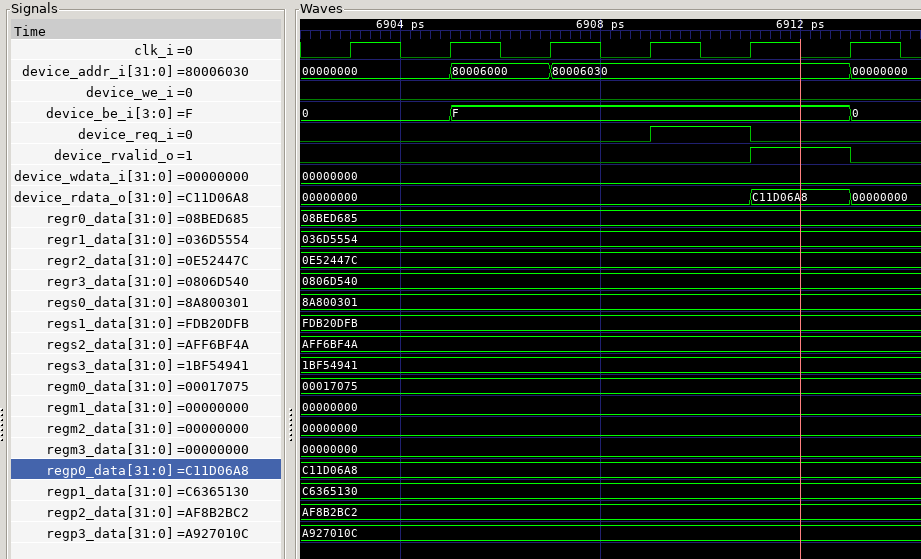
The following figure shows a simulation that captures a complete
poly1305 operation in hardware as three message blocks. The timing
diagram monitors the bus interface (device_..) and the
memory-mapped registers. Next, we outline the timing behavior of
an IBEX write bus cycle and an IBEX read bus cycle.
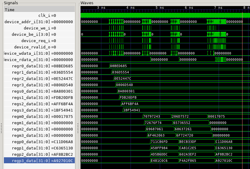
The IBEX bus cycle
Writing to the coprocess takes two clock cycles. In the first cycle,
the IBEX asserts the address, device request signal, write control
signal, byte-enable signal, and value to write. The coprocessor must
decode the bus in one cycle and respond with an rvalid in the next
cycle. At the same time, the memory-mapped register is updated.
Eventually, the IBEX removes the address and other bus controls.
Reading from the coprocessor takes two cycles. In the first cycle, the
IBEX asserts the address, device request signal, de-asserts write
control signal, asserts the byte-enable signal. The coprocessor must
decode the bus in one cycle and respond with an rvalid in the next
cycle. At that time, the output data bus must be dirven. Eventually,
the IBEX removes the address and other bus controls.
Synthesis and Layout
Important
Do not start working on this section until you have a completely working Verilator simulation. This means that you must first obtain a correct simulation that demonstrates that your hardware poly1305 computes the same tag value as the poly1305 reference software.
Once you have achieved that milestone, you can then move to coprocessor synthesis. You will receive a repository that is fully prepared to synthesize and layout your design, and where you only have to add RTL.
To clone that additional repository, accept the following Github classroom link: https://classroom.github.com/a/0BlhqXyC
Clone the resulting repository, which is called final-project-synthesis-userid You need at least one repo per team, although both team members can accept and clone the repository.
The following starts after you have cloned the synthesis repository, which follows the same structure as the standard ECE574 flow.
Step 1: Copy and configure RTL
Your first step is the copy the RTL of the coprocessor from your final-project
repo to the rtl subdirectory. The synthesis repo is configured for
a toplevel module name poly1305top. If you change this, you will need to
adjust the Makefiles as needed.
For example, in my case, this directory looks as follows.
[pschaumont@arc-schaumont-class-vm rtl]$ ls
poly1305.sv  poly1305top.sv  processblock.sv
Step 2: Run an RTL simulation
As a sanity check, you will run and RTL simulation in sim. Make sure
to update the Makefile so that all files are included in the simulation.
Next, inspect the testbench tb.sv, which runs an access sequence through
the coprocessor. You can use writebus and readbus tasks to quickly
generate bus cycles. The testbench runs through three message blocks and then
checks the resulting tag. Depending on how you have defined the memory-mapped
registers, small changes to tb.sv may be needed.
Afterwards you can just type make. If the testbench completes successfully,
you will see: Test Vector Passes.
Step 3: RTL synthesis
Next, go to the syn directory, update the Makefile to include all files
of your coprocessor and run logic synthesis. Inspect the synthesis results
in reports and find the area of your design.
Important
1. If your design exceeds 25K cells, the layout of your coprocessor will be lengthy, and I recommend that you perform these runs at night only.
2. You can relax the cycle constraint of your implementation
for example from CLOCKPERIOD=4 to CLOCKPERIOD=10. A relaxed
timing constraint will make synthesis complete faster. If your
coprocessor has negative slack (reports/poly1305top_report_timing.rpt),
you will need to relax the clock period.
3. Make sure to check your coprocessor for latches (grep LAT
outputs/poly1305top_netlist.v). No latches should exist in the final
design.
Step 4: Static Timing Analysis
Next, go to the sta directory, and run a static timing analysis.
Make sure that your design is correct for setup timing. Since we have
not defined timing constraints for asynchronous inputs (reset), you
can ignore timing problems from reset.
Step 5: Gate Level Simulation (optional)
Next, go to the glsim directory and perform gate-level simulation
using post-synthesis timing. If you modified the RTL testbench for
your coprocessor design, you may also need similar changes to the
gate level testbench.
make sim-postsyn
or
make sim-postsyn-gui
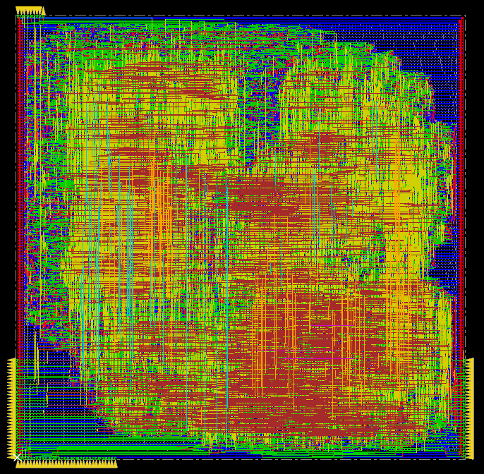
Step 6: Layout
Next, go to the layout directory and create the layout.
The chip IO pinout is already defined in chip/chip.io (you
may change it, if needed or desired).
Make sure that the Makefile reflects the complete set
of RTL files for your coprocessor. Then, build the layout.
make syn
make layout
If you succeed with the layout, you should be able to produce a final layout of your complete coprocessor design.
Step 7: Post Layout Simulation (optional)
Next, go back to the glsim directory and perform gate-level simulation
using post-layout timing.
make sim-postlayout
or
make sim-postlayout-gui
Step 8: Collect Design Data
If you have completed all design steps described above, congratulations, you are done! During the design steps, a great number of design reports and diagnostic information was generated. Go back and collect that data for your presentation.
The
syndirectory contain area, timing and power estimates from logic synthesisThe
stadirectory contains the critical path definition for the selected clock periodThe
layout/reportsamdlayout/reports/STAcontains post-layout design data related to area, power, timing, and clock tree.
Project Presentation
This section summarizes the requirements for the project presentation.
If you participated in the ‘Tiny Tapeout’ projects
Your final presentation will consist of a 20 minute powerpoint presentation on your design. Discuss the application in detail, since the rest of the class did not hear about your application yet. Put special emphasis on the following two aspects related to the design:
Dealing with area and performance constraints.
Dealing with design verification, either through simulation or else through prototyping.
Deliverables for your final project include the following.
The github repository of your tiny tapeout submission
Your slide deck must be submitted to the instructor before the presentation on 11 December.
If you participated in the ‘poly1305’ project in the in-person course
The deliverables for your final project include the following. The slide deck and excel sheet must be emailed to the instructor before the start of your presentation. One email per team is sufficient. Make sure to indicate the names of the students participating in the team.
The gtihub repository for the IBEX Verilator based cosimulation
The github repository for the synthesis of your coprocessor
The slide deck of your final presentation
The following excel sheet filled out with data statistics of your design:
project-metrics.xlsx
Your final presentation will consist of a 15-minute or 10-minute powerpoint presentation on your design. The schedule will show if you are going to talk for 15 or 10 minutes. In your talk, you have to highlight the main design phases of your design, depending on how far you were able to finish the design. There are four design phases:
1/ RTL coding corresponding to the ‘RTL’ section in the Projects Metrics. You have made an initial architecture design for the accelerator, along with RTL coding. In your slides, demonstrate the design hierarchy and major design properties such as the number of data multipliers, and the clock cycle latency for a modular multiplication.
2/ SIMULATION which includes (a) simulation of the full coprocessor in the IBEX Verilator system simulation, and (b) stand-alone Verilog simulation of the coprocessor as it is moved to synthesis. Both simulations need to compute the correct Poly1305 Tag before moving futher into synthesis.
3/ SYNTHESIS which includes RTL synthesis of your design (the ‘syn’ step of the ECE574 flow). Report the major properties of your design including the achieved clock period, slack, leaf instance count (number of standard cells), the number of flip-flops, and the active cell area. You may report these numbers for multiple clock periods, if you want to showcase the area/delay tradeoff in your design. The design delay (critical path * design latency) and the active cell area will be used to plot your design in a global Pareto plot.
4/ LAYOUT which includes layout of your design (the ‘layout’ step of the ECE574 flow). Report the major properties of your design: the clock period, slack, leaf instance count including physical cells, total area of standard cells, and gate density. Consult the excel sheet for guidance on where to take all these measurements.
If you participated in the ‘poly1305’ project in the online class
The deliverables for your final project include the following. The slide deck and excel sheet must be emailed to the instructor together with the video. The submission deadline is Friday 12/13, 11:59PM. One email per team is sufficient. Make sure to indicate the names of the students participating in the team.
The github repository for the IBEX Verilator based cosimulation
The github repository for the synthesis of your coprocessor
The slide deck of your final presentation
The following excel sheet filled out with data statistics of your design:
project-metrics.xlsx
Your final presentation will consist of a 10-minute video presentation on your design. In your talk, you have to highlight the main design phases of your design, depending on how far you were able to finish the design. Refer to the section above for a description of each phase, including RTL, SIMULATION, SYNTHESIS and LAYOUT.