Attention
This document was last updated Nov 25 24 at 21:59
Optimizing Area and Timing
Important
The purpose of this lecture is as follows.
To explore the impact of optimization on design cost factors (gate count, performance, layout area) for a concrete design
To apply two techniques that help in building high-speed hardware
To apply two techniques that help in building low-area hardware
To discuss Verilog coding and testbench design for all these cases
Important
The designs discussed in this lecture are on https://github.com/wpi-ece574-f24/ex-layout-avg64
Moving Average Application
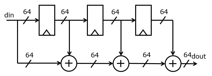
We will study a concrete design consisting of a moving-average filter application with a 64-bit wordlength. The filter adds up the last 4 samples that have been entered at the din input. When two 64-bit numbers are added, the carry-out bit is thrown out, and only the lower 64 bits are kept.
This implementation exhibits the following characteristics.
The inputs and outputs are produced at a rate of 1 data element per clock cycle. Thus, the data introduction interval of the reference implementation is one per clock cycle.
There is a combinational path that runs from input to output through three 64-bit additions. The latency of the implementation, counted in clock cycles, is 0 cycles. That is, if the input is applied at
 (ns), then the output will be ready at
  (ns), with
  the time of the combinational path through three 64-bit additions. Obviously, to avoid a timing path violation on a clock period of
  , we must ensure that
  . If the input delay constraint on din is
  , and the output delay constraint on dout is
  , then we must ensure that
  .
.The input is captured into a register which forms part of a register delay chain. The combinational delay along the chain is very small, and defined by the clock-to-Q delay of the register. Therefore, it’s reasonable to assume that the slowest path in the overall design will be dominated by three sequential additions. Nevertheless, one must keep in mind that the chain of 64-bit adders enables considerable parallellism, as the adder chain sums up four indepent numbers with are available at the start of the cycle (plus the input delay for din, plus the clock-to-Q delay for the registers).
 1module movavg(
 2    input logic clk,
 3    input logic reset,
 4    input logic [63:0] din,
 5    output logic [63:0] dout
 6);
 7
 8   logic [63:0]         tap1, tap1_next;
 9   logic [63:0]         tap2, tap2_next;
10   logic [63:0]         tap3, tap3_next;
11
12   always_ff @(posedge clk) begin
13      if (reset) begin
14         tap1 <= 64'h0;
15         tap2 <= 64'h0;
16         tap3 <= 64'h0;
17      end else begin
18         tap1 <= tap1_next;
19         tap2 <= tap2_next;
20         tap3 <= tap3_next;
21      end
22   end
23
24   logic [63:0] doutreg;
25
26   always_comb begin
27      doutreg   = din + tap1 + tap2 + tap3;
28      tap1_next = din;
29      tap2_next = tap1;
30      tap3_next = tap2;
31   end
32
33   assign dout = doutreg;
34
35endmodule
The correctness of the design is evaluated using a testbench that feeds in random values. The testbench performs a parallel computation while feeding random values, so that the correctness of the module implementation is verified.
In the following testbench, pay special attention to the timing of the testbench. Since the DUT has no data-ready signal, the testbench is sensitive to the time when the output DUT.dout is read.
(line 7) We apply a 10ns clock. At this point, we are looking for functional timing verification, so the period is an arbitrary but convenient number.
(line 33) We use a one-cycle reset sequence and start applying inputs from cycle 2. The reference values chk_tap1, chk_tap2, chk_tap3 are reset simultaneously with the module.
(Line 42) Each clock cycle, a new vector is applied. The input to the DUT is provided with a tiny delay to the module inputs. This ensures that the inputs are not changing exactly at the clock edge. While an RTL simulation suffers no hold timing effects, there may still occur non-deterministic behavior when multiple variables change at the same simulation timestamp. In this case, we have to make sure that the registers in the DUT are updated before din changes value.
(Line 54) We assert the outputs at the end of the clock period, just before the clock edge.
(Line 60) We update the delay line after the output assertion is complete. Then, we await the next clock edge and move to the next input test vector.
 1`timescale 1ns/1ps
 2`define CLOCKPERIOD 10
 3
 4module tb;
 5   logic clk, reset;
 6
 7   always
 8     begin
 9       clk = 1'b0;
10       #(`CLOCKPERIOD/2);
11       clk = 1'b1;
12       #(`CLOCKPERIOD/2);
13     end
14
15   logic [63:0] din;
16   logic [63:0] dout;
17
18   movavg DUT(.clk(clk),
19              .reset(reset),
20              .din(din),
21              .dout(dout)
22              );
23
24   logic [63:0] chk_tap3;
25   logic [63:0] chk_tap2;
26   logic [63:0] chk_tap1;
27   logic [63:0] chk_din;
28   logic [63:0] chk_dout;
29
30   initial
31     begin
32        reset = 1'b1;
33        @(negedge clk);
34        reset = 1'b0;
35        chk_tap1 = 0;
36        chk_tap2 = 0;
37        chk_tap3 = 0;
38        din      = 0;
39
40        @(posedge clk);
41
42        while (1)
43          begin
44
45             #1; // making sure we assign new inputs just after the clock edge
46
47             din[31:0]  = $random;
48             din[63:32] = $random;
49
50             chk_din = din;
51
52             #(`CLOCKPERIOD - 1);
53
54             chk_dout = chk_din + chk_tap3 + chk_tap2 + chk_tap1;
55
56             $display("%t out %h expected %h OK %d", $time, dout, chk_dout, dout == chk_dout);
57             // $display("%t DUT in %h taps %h %h %h",  $time, DUT.din, DUT.tap1, DUT.tap2, DUT.tap3);
58             // $display("%t CHK in %h taps %h %h %h",  $time, chk_din, chk_tap1, chk_tap2, chk_tap3);
59
60             chk_tap3 = chk_tap2;
61             chk_tap2 = chk_tap1;
62             chk_tap1 = chk_din;
63             @(posedge clk);
64
65          end
66     end
67
68   initial
69     begin
70        repeat(256)
71          @(posedge clk);
72        $finish;
73     end
74
75endmodule
FAST design strategy #1: Pipelining
The first design strategy to improve performance of the reference design is to introduce pipeline registers. Because the design does not have a latency requirement, an arbitrary number of pipeline registers can be inserted.
The main challenge for pipelining is to ensure that pipeline registers are inserted consistently, i.e. according to the rules of retiming as discussed in our lecture on Timing. Because the reference design has no feedback loops, the insertion of pipeline registers can be done by leveling of the circuit graph. The expected critical path of the design runs through three sequential adders. Therefore, these adders are isolated by two pipeline registers.
We do not insert a pipeline register at the input (din) or the output (dout) because we are assuming that the input delay and the output delay are both 0. When a different constraint would be chosen, this may lead to the insertion of an additional pipeline register at din or dout.
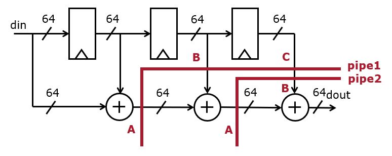
Furthermore, we do not insert a pipeline register within the adder, although it is perfectly feasible to pipeline the adder itself as well:
In the overall pipelined design, notice how the insertion of a pipeline level
implies the insertion of multiple 64-bit registers. For example, the first
pipeline level leads to three registers: pipe1a at the output of the
first adder, pipe1b at the input of the second adder, and pipe1c at
the output of the third tap.
We can thus rewrite the Verilog description while inserting these additional registers in the computation flow.
 1`define WL 63
 2`define WL1 64
 3
 4module movavg(input wire         clk,
 5              input wire         reset,
 6              input wire [`WL:0]  din,
 7              output wire [`WL:0] dout);
 8
 9   reg [`WL:0]                    tap1, tap1_next;
10   reg [`WL:0]                    tap2, tap2_next;
11   reg [`WL:0]                    tap3, tap3_next;
12
13   reg [`WL:0]         pipe1a, pipe1a_next;
14   reg [`WL:0]         pipe1b, pipe1b_next;
15   reg [`WL:0]         pipe1c, pipe1c_next;
16   reg [`WL:0]         pipe2a, pipe2a_next;
17   reg [`WL:0]         pipe2b, pipe2b_next;
18
19   always @(posedge clk)
20     begin
21        if (reset)
22          begin
23             tap1 <= `WL1'h0;
24             tap2 <= `WL1'h0;
25             tap3 <= `WL1'h0;
26             pipe1a <= `WL1'h0;
27             pipe1b <= `WL1'h0;
28             pipe1c <= `WL1'h0;
29             pipe2a <= `WL1'h0;
30             pipe2b <= `WL1'h0;
31          end
32        else
33          begin
34             tap1   <= tap1_next;
35             tap2   <= tap2_next;
36             tap3   <= tap3_next;
37             pipe1a <= pipe1a_next;
38             pipe1b <= pipe1b_next;
39             pipe1c <= pipe1c_next;
40             pipe2a <= pipe2a_next;
41             pipe2b <= pipe2b_next;
42          end
43     end // always @ (posedge clk)
44
45   reg [`WL:0] doutreg;
46
47   always @(*)
48     begin
49        pipe1a_next = din + tap1;
50        pipe1b_next = tap2;
51        pipe1c_next = tap3;
52        pipe2a_next = pipe1a + pipe1b;
53        pipe2b_next = pipe1c;
54        doutreg     = pipe2a + pipe2b;
55        tap1_next   = din;
56        tap2_next   = tap1;
57        tap3_next   = tap2;
58     end
59
60   assign dout = doutreg;
61
62endmodule
Attention
The delay of the pipelined design will be given by the critical path, since a new result is computed every clock cycle.
For a pipelined design, we have to adjust the testbench so that it deals with the increased latency of the design. With two pipeline registers, the result is available two clock cycles later. Additionally, the testbench has to take into account that a pipelined design will complete several sums at the same time.
(Line 57) The testbench keeps track of the two previous results,
pp_chk_doutandp+chk_doutwhile computing the current result,chk_dout.(Line 62) The result is tested from the first cycle. This implies that we can expect the first two results to be wrong. So, we would check OK only from the third result produced.
 1`timescale 1ns/1ps
 2`define CLOCKPERIOD 10
 3
 4module tb;
 5   logic clk, reset;
 6
 7   always
 8     begin
 9       clk = 1'b0;
10       #(`CLOCKPERIOD/2);
11       clk = 1'b1;
12       #(`CLOCKPERIOD/2);
13     end
14
15   logic [63:0] din;
16   logic [63:0] dout;
17
18   movavg DUT(.clk(clk),
19              .reset(reset),
20              .din(din),
21              .dout(dout)
22              );
23
24   logic [63:0] chk_tap3;
25   logic [63:0] chk_tap2;
26   logic [63:0] chk_tap1;
27   logic [63:0] chk_din;
28   logic [63:0] chk_dout;
29   logic [63:0] p_chk_dout;
30   logic [63:0] pp_chk_dout;
31
32   initial
33     begin
34        reset = 1'b1;
35        @(negedge clk);
36        reset = 1'b0;
37        chk_tap1 = 0;
38        chk_tap2 = 0;
39        chk_tap3 = 0;
40        din      = 0;
41
42        @(posedge clk);
43
44        while (1)
45          begin
46
47             #1; // making sure we assign new inputs just after the clock edge
48
49             din[31:0]  = $random;
50             din[63:32] = $random;
51
52             chk_din = din;
53
54             #(`CLOCKPERIOD - 1);
55
56             // This delay ensures the tested output matches the pipelined output (2 pipe    stages)
57             pp_chk_dout = p_chk_dout;
58             p_chk_dout = chk_dout;
59             chk_dout = chk_din + chk_tap3 + chk_tap2 + chk_tap1;
60
61             $display("%t out %h expected %h OK %d", $time, dout, pp_chk_dout, dout ==    pp_chk_dout);
62             $display("%t CHK in %h taps %h %h %h -> %h",  $time, chk_din, chk_tap1,    chk_tap2, chk_tap3, chk_dout);
63
64             chk_tap3 = chk_tap2;
65             chk_tap2 = chk_tap1;
66             chk_tap1 = chk_din;
67             @(posedge clk);
68
69          end
70     end
71
72   initial
73     begin
74        repeat(256)
75          @(posedge clk);
76        $finish;
77     end
78
79endmodule
Here are the first few lines of the testbench output demonstrating the latency effect. Note that the third result b9594e719d53863a, ie. the output after three inputs, is only checked when the fifth input is read in at timestamp 65000.
25000 out 0000000000000000 expected xxxxxxxxxxxxxxxx OK x
25000 CHK in c0895e8112153524 taps 0000000000000000 0000000000000000 0000000000000000 -> c0895e8112153524
35000 out 0000000000000000 expected xxxxxxxxxxxxxxxx OK x
35000 CHK in b1f056638484d609 taps c0895e8112153524 0000000000000000 0000000000000000 -> 7279b4e4969a0b2d
45000 out c0895e8112153524 expected c0895e8112153524 OK 1
45000 CHK in 46df998d06b97b0d taps b1f056638484d609 c0895e8112153524 0000000000000000 -> b9594e719d53863a
55000 out 7279b4e4969a0b2d expected 7279b4e4969a0b2d OK 1
55000 CHK in 89375212b2c28465 taps 46df998d06b97b0d b1f056638484d609 c0895e8112153524 -> 4290a08450160a9f
65000 out b9594e719d53863a expected b9594e719d53863a OK 1
65000 CHK in 06d7cd0d00f3e301 taps 89375212b2c28465 46df998d06b97b0d b1f056638484d609 -> 88df0f103ef4b87c
FAST design strategy #2: Unfolding
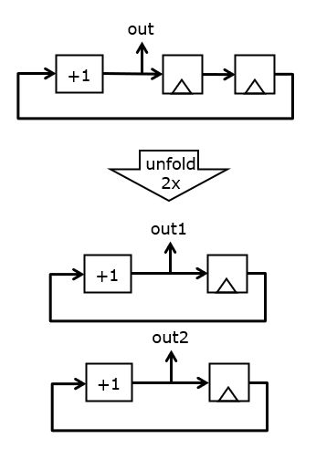
An alternate strategy to improve design performance is to exploit the parallellism of hardware and remove the input/output constraint of a single data item per cycle. This strategy is called unfolding. Unfolding is more than simply parallellizing. For example, simply doubling the averager is not a correct implementation of the averaging algorithm, because that implementation would compute the average on two independent streams. In unfolding, we perform computations on a single stream of data items which are delivered in groups of n data items at a time.
The following example illustrates this concept. A simple counter circuit counts at a rate of one per clock cycle. The 2x unfolded version of this counter will produce two outputs per clock cycle, n and n+1. We have this by doubling the combinational hardware. However, the state variables of the unfolded circuit are identical to those of the original circuit: there is still one single register.
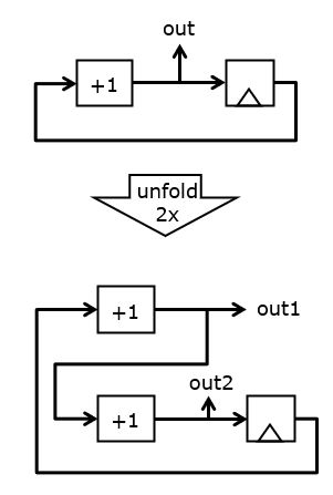
The unfolding transformation is general, and applies to any circuit. For example, assume we have a counter circuit with two back-to-back registers. If the initial state of the registers is zero, then the sequence of values produced at the output will be 1, 1, 2, 2, 3, 3, 4, 4, and so forth. The 2x unfolded version of this circuit is shown below that. It uses two incrementer circuits, and the state variables of the original circuit are distributed over the unfolded circuit. It’s easy to see that this circuit produced the same outputs as the original circuit, but in pairs of two: (1,1), (2,2), (3,3), ..
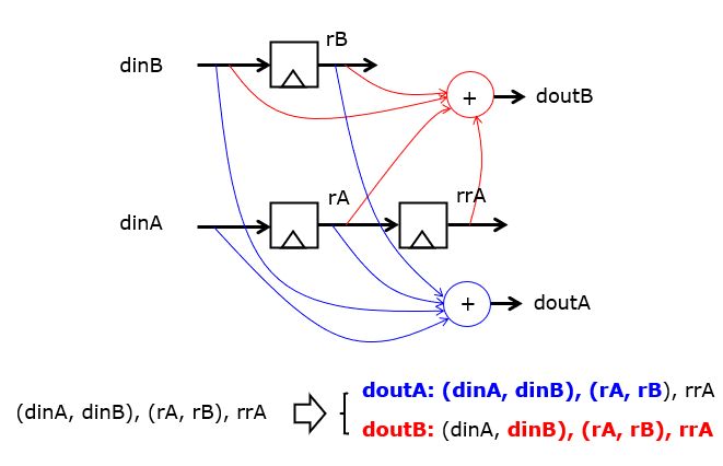
It is possible to derive systematic unfolding rules for arbitrary circuits, but since the averager is sufficiently small and simple, we can attempt to derive a 2x unfolded version by hand. The unfolded version of the averager reads in pairs of data (dinA, dinB) and produced pairs of output data (doutA, doutB). The output data is the sum of the last four data items in the stream. For example, if the stream consists of the tuples (dinA1, dinB1), (dinA2, dinB2), (dinA3, dinB3) (with dinA1 the most recent), then the outputs are defined by (doutA = dinA1 + dinB1 + dinA2 + dinB2) and (doutB = dinB1 + dinA2 + dinB2 + dinA3). Graphically, this leads to the unfolded circuit we aim to create. Notice that the number of state variables is the same as the original circuit (3 registers) while the logic has doubled.
 1module movavg(input wire         clk,
 2              input wire     reset,
 3              input wire [63:0]  dinA,
 4              input wire [63:0]  dinB,
 5              output wire [63:0] doutA,
 6              output wire [63:0] doutB);
 7
 8   reg [63:0]             tap1, tap1_next;
 9   reg [63:0]             tap2, tap2_next;
10   reg [63:0]             tap3, tap3_next;
11
12   always @(posedge clk)
13     begin
14    if (reset)
15      begin
16         tap1 <= 64'h0;
17         tap2 <= 64'h0;
18         tap3 <= 64'h0;
19      end
20    else
21      begin
22         tap1 <= tap1_next;
23         tap2 <= tap2_next;
24         tap3 <= tap3_next;
25      end
26     end // always @ (posedge clk)
27
28   reg [63:0] doutregA;
29   reg [63:0] doutregB;
30
31   always @(*)
32     begin
33       doutregA   = dinA + dinB + tap1 + tap2;
34       doutregB   = dinB + tap1 + tap2 + tap3;
35       tap1_next  = dinA;
36       tap2_next  = dinB;
37       tap3_next  = tap1;
38     end
39
40   assign doutA = doutregA;
41   assign doutB = doutregB;
42
43endmodule
Attention
The delay of the unfolded design will be given by the critical path divided by the unfolding factor (2). Each clock cycle, two new results are computed.
The testbench of this design will have to reflect the double-rate nature of the hardware, and hence verify two outputs per iteration. The latency of the design is still 0 clock cycles, as with the original design. The test bench verification does not implement the unfolded design, but rather implements the original design working at twice the speed. That is, each loop iteration, two new items are inserted into the delsy line and two outputs are computed.
(line 61-62): the first (oldest) element is inserted into the delay line
(line 66-67): Two consecutive outputs of the moving averager are computed
 1`timescale 1ns/1ps
 2`define CLOCKPERIOD 10
 3
 4module tb;
 5   logic clk, reset;
 6
 7   always
 8     begin
 9       clk = 1'b0;
10       #(`CLOCKPERIOD/2);
11       clk = 1'b1;
12       #(`CLOCKPERIOD/2);
13     end
14
15   logic [63:0] dinA;
16   logic [63:0] doutA;
17   logic [63:0] dinB;
18   logic [63:0] doutB;
19
20   movavg DUT(.clk(clk),
21              .reset(reset),
22              .dinA(dinA),
23              .dinB(dinB),
24              .doutA(doutA),
25              .doutB(doutB)
26              );
27
28   logic [63:0] chk_tap4;
29   logic [63:0] chk_tap3;
30   logic [63:0] chk_tap2;
31   logic [63:0] chk_tap1;
32   logic [63:0] chk_dinA;
33   logic [63:0] chk_doutA;
34   logic [63:0] chk_dinB;
35   logic [63:0] chk_doutB;
36
37   initial
38     begin
39        reset = 1'b1;
40        @(negedge clk);
41        reset = 1'b0;
42        chk_tap1 = 0;
43        chk_tap2 = 0;
44        chk_tap3 = 0;
45        dinA     = 0;
46        dinB     = 0;
47
48        @(posedge clk);
49
50        while (1)
51          begin
52
53             #1; // making sure we assign new inputs just after the clock edge
54
55             dinA[31:0]  = $random;
56             dinA[63:32] = $random;
57
58             dinB[31:0]  = $random;
59             dinB[63:32] = $random;
60
61             chk_dinB = dinB;
62             chk_dinA = dinA;
63
64             #(`CLOCKPERIOD - 1);
65
66             chk_doutA = chk_dinA + chk_dinB + chk_tap1 + chk_tap2;
67             chk_doutB = chk_dinB + chk_tap1 + chk_tap2 + chk_tap3;
68
69             $display("A %t out %h expected %h OK %d", $time, doutA, chk_doutA, doutA == chk_doutA);
70             $display("B %t out %h expected %h OK %d", $time, doutB, chk_doutB, doutB == chk_doutB);
71             // $display("%t DUT in %h taps %h %h %h",  $time, DUT.din, DUT.tap1, DUT.tap2, DUT.tap3);
72             // $display("%t CHK in %h taps %h %h %h",  $time, chk_din, chk_tap1, chk_tap2, chk_tap3);
73
74             chk_tap3 = chk_tap1;
75             chk_tap2 = chk_dinB;
76             chk_tap1 = chk_dinA;
77
78             @(posedge clk);
79
80          end
81     end
82
83   initial
84     begin
85        repeat(256)
86          @(posedge clk);
87        $finish;
88     end
89
90endmodule
SMALL design strategy #1: Sequentializing
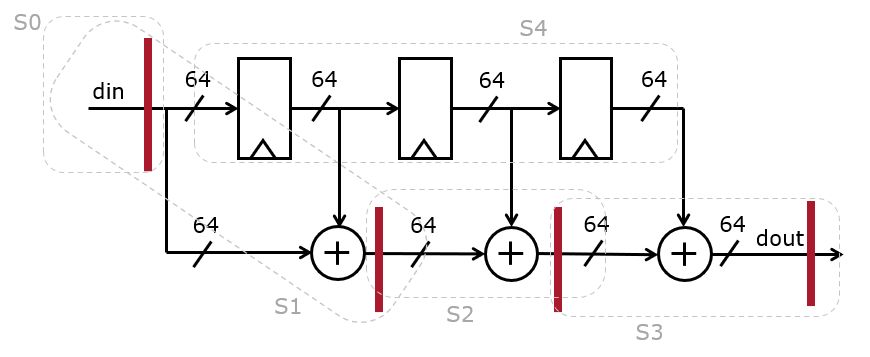
To reduce the area of a hardware design, we have to reuse hardware elements over multiple clock cycles. An obvious candidate for reuse is the 64-bit adder. The flow graph of the average is partitioned in clusters that contain simular operations. At the edge of a cluster, a register is placed to carry signals over to the next clock cycle.
(Line 48-75) We use a 5-state FSM that reads the input, accumulates all the taps, and finally shifts the taps and produces the output
The level of area reduction depends on two things. First, the synthesis tools have to realize that the 64-bit addition can be reused over different FSM states. Second, the area saved by sharing the adder hardware must be larger than the area overhead added by the sharing support hardware. This includes the finite state machine, the accmulator register (line 11), and the multiplexers (invisible in the RTL!). This is no small requirement, and we will see that this overhead is significant.
 1module movavg(input logic         clk,
 2              input logic         reset,
 3              input logic [63:0]  din,
 4              output logic [63:0] dout,
 5              output logic        read
 6              );
 7
 8   typedef enum         logic [3:0] {
 9                                     S0 = 4'b0000,
10                                     S1 = 4'b0001,
11                                     S2 = 4'b0010,
12                                     S3 = 4'b0011,
13                                     S4 = 4'b0100
14                                     } state_t;
15
16   logic [63:0]  tap1, tap1_next;
17   logic [63:0]  tap2, tap2_next;
18   logic [63:0]  tap3, tap3_next;
19
20   state_t state, state_next;
21   logic [63:0]  acc, acc_next;
22
23   always_ff @(posedge clk)
24     begin
25        if (reset)
26          begin
27             tap1 <= 64'h0;
28             tap2 <= 64'h0;
29             tap3 <= 64'h0;
30             acc  <= 64'h0;
31             state <= S0;
32          end
33        else
34          begin
35             tap1  <= tap1_next;
36             tap2  <= tap2_next;
37             tap3  <= tap3_next;
38             acc   <= acc_next;
39             state <= state_next;
40          end
41     end
42
43   logic [63:0] doutreg;
44   logic        readreg;
45
46   always @(*)
47     begin
48        state_next = state;
49        acc_next   = acc;
50        tap1_next  = tap1;
51        tap2_next  = tap2;
52        tap3_next  = tap3;
53        doutreg    = 64'h0;
54        readreg    = 1'b0;
55        case (state)
56          S0:
57            begin
58               acc_next   = din;
59               readreg    = 1'b1;
60               state_next = S1;
61            end
62          S1:
63            begin
64               acc_next   = acc + tap1;
65               state_next = S2;
66            end
67          S2:
68            begin
69               acc_next   = acc + tap2;
70               state_next = S3;
71            end
72          S3:
73            begin
74               acc_next   = acc + tap3;
75               state_next = S4;
76            end
77          S4:
78            begin
79               doutreg    = acc;
80               tap1_next  = din;
81               tap2_next  = tap1;
82               tap3_next  = tap2;
83               state_next = S0;
84            end
85          default:
86            state_next = S0;
87        endcase
88     end
89
90   assign dout = doutreg;
91   assign read = readreg;
92
93endmodule
Attention
The delay of the sequential design equals the critical path times the number of clock cycles required to compute the output dout (5).
The testbench of the sequential design is derived from the original testbench and simply increases the latency of the design by 4 cycles. We have also introduced an additional synchronization signal, ready, which indicates when the FSM is in state S0. In that state, the new input is read in to the delay line.
 1`timescale 1ns/1ps
 2`define CLOCKPERIOD 10
 3
 4module tb;
 5   logic clk, reset;
 6
 7   always
 8     begin
 9       clk = 1'b0;
10       #(`CLOCKPERIOD/2);
11       clk = 1'b1;
12       #(`CLOCKPERIOD/2);
13     end
14
15   logic [63:0] din;
16   logic [63:0] dout;
17   logic        read;
18
19   movavg DUT(.clk(clk),
20              .reset(reset),
21              .din(din),
22              .dout(dout),
23              .read(read)
24              );
25
26   logic [63:0] chk_tap3;
27   logic [63:0] chk_tap2;
28   logic [63:0] chk_tap1;
29   logic [63:0] chk_din;
30   logic [63:0] chk_dout;
31
32   initial
33     begin
34        reset = 1'b1;
35        @(negedge clk);
36        reset = 1'b0;
37        chk_tap1 = 0;
38        chk_tap2 = 0;
39        chk_tap3 = 0;
40        din      = 0;
41
42        while (read == 1'b0) // wait until computation can start
43          @(posedge clk);
44
45        while (1)
46          begin
47
48             #1; // making sure we assign new inputs just after the clock edge
49
50             din[31:0]  = $random;
51             din[63:32] = $random;
52
53             chk_din = din;
54
55             repeat(4)
56               @(posedge clk); // wait until FSM complete
57
58             #(`CLOCKPERIOD - 2);
59
60             chk_dout = chk_din + chk_tap3 + chk_tap2 + chk_tap1;
61
62             $display("%t out %h expected %h OK %d", $time, dout, chk_dout, dout == chk_dout);
63//           $display("%t DUT in %h taps %h %h %h",  $time, DUT.din, DUT.tap1, DUT.tap2, DUT.tap3);
64//           $display("%t CHK in %h taps %h %h %h",  $time, chk_din, chk_tap1, chk_tap2, chk_tap3);
65
66             chk_tap3 = chk_tap2;
67             chk_tap2 = chk_tap1;
68             chk_tap1 = chk_din;
69             @(posedge clk);
70
71          end
72     end
73
74   initial
75     begin
76        repeat(256)
77          @(posedge clk);
78        $finish;
79     end
80
81endmodule
SMALL design strategy #2: Bit-serializing
The second strategy towards small area is to take the hardware reuse concept to the extreme, and transform the 64-bit averager to a bit-serial design. The basic components of the design are easy to transform to bit-serial circuits:
A 64-bit adder becomes a 1-bit bit-serial adder
A 64-bit tap register becomes a 64-bit shift register (a 64-position 1-bit FIFO)
Parallel inputs and outputs are created using appropriate parallel to serial and serial to parallel registers
A challenge of bit-serial design is the controller, which needs to create a sync signal with a duty cycle of 1/64. The phase of the sync signal changes with the position of the bit-serial operator in the overall design.
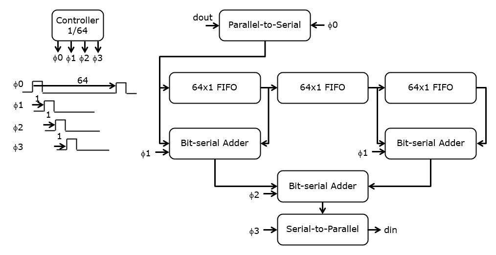
The advantage of bit-serialization over sequentializing is that we can get rid of most multiplexers by ensuring that the data arrives always just-in-time. The latency of this design is a little more complicated; every 64 clock cycles, a new result is produced. However, the output is offset by 4 clock cycles from the input due to the phase delay inserted during bit-serial computation.
The controller is implemented as a 6-bit cyclic counter. The phase signals
 are derived from this counter by
decoding the proper counter state. An alternate implementation would by
a 64-bit circular shift register – which is probably larger than this solution
due to the relatively large size of a flip-flop cell.
are derived from this counter by
decoding the proper counter state. An alternate implementation would by
a 64-bit circular shift register – which is probably larger than this solution
due to the relatively large size of a flip-flop cell.Three additional modules are used to create this implementation: a parallel-to-serial converter, a serial-to-parallel converter and a bit-serial adder.
The tap registers from earlier implementations are reused as 64x1 FIFO registers.
  1 module movavg(input wire         clk,
  2               input wire     reset,
  3               input wire [63:0]  din,
  4               output wire [63:0] dout);
  5
  6    reg [63:0]             tap1, tap1_next;
  7    reg [63:0]             tap2, tap2_next;
  8    reg [63:0]             tap3, tap3_next;
  9
 10    reg [5:0]              ctr, ctr_next;
 11
 12    always @(posedge clk)
 13      begin
 14        if (reset)
 15          begin
 16             tap1 <= 64'h0;
 17             tap2 <= 64'h0;
 18             tap3 <= 64'h0;
 19             ctr <= 5'd0;
 20          end
 21        else
 22          begin
 23             tap1 <= tap1_next;
 24             tap2 <= tap2_next;
 25             tap3 <= tap3_next;
 26             ctr  <= ctr_next;
 27          end
 28       end // always @ (posedge clk)
 29
 30    // controller
 31    reg ctl0, ctl1, ctl2, ctl3, ctl4;
 32    always @(*)
 33      begin
 34        ctr_next = ctr + 6'b1;
 35        ctl0 = (ctr == 6'd0);
 36        ctl1 = (ctr == 6'd1);
 37        ctl2 = (ctr == 6'd2);
 38        ctl3 = (ctr == 6'd3);
 39        ctl4 = (ctr == 6'd4);
 40      end
 41
 42    // first stage: parallel to serial conversion
 43    wire din_s;
 44    ps stage1(din, ctl0, clk, din_s);
 45
 46    // second stage: delay line
 47    always @(*)
 48      begin
 49        tap1_next = {din_s, tap1[63:1]};
 50        tap2_next = {tap1[0], tap2[63:1]};
 51        tap3_next = {tap2[0], tap3[63:1]};
 52      end
 53
 54    // third stage: first set of adders
 55    wire a1_s, a2_s;
 56    serialadd a1(din_s,    tap1[0], a1_s, ctl1, clk);
 57    serialadd a2(tap2[0],  tap3[0], a2_s, ctl1, clk);
 58
 59    // fourth stage: second adder
 60    wire a3_s;
 61    serialadd a3(a1_s, a2_s, a3_s, ctl2, clk);
 62
 63    // final stage: s/p converter
 64    sp stage9(a3_s, ctl3, clk, dout);
 65
 66 endmodule
 67
 68 module ps(input wire[63:0] a,
 69           input wire  sync,
 70           input wire  clk,
 71           output wire as);
 72
 73    reg [63:0]         ra;
 74
 75    always @(posedge clk)
 76      if (sync)
 77        ra <= a;
 78      else
 79        ra <= {1'b0, ra[63:1]};
 80
 81    assign as = ra[0];
 82
 83 endmodule // ps
 84
 85 module sp(input wire as,
 86           input wire         sync,
 87           input wire         clk,
 88           output wire [63:0] a);
 89
 90    reg [63:0]            ra;
 91
 92    always  @(posedge clk)
 93      ra <= {as, ra[63:1]};
 94
 95    assign a  = sync ? ra : 8'b0;
 96
 97 endmodule // sp
 98
 99 module serialadd(input wire a, input wire b, output wire s,
100                  input wire sync, input wire clk);
101
102    reg              carry, q;
103
104    always @(posedge clk)
105      if (sync)
106        begin
107           carry <= a & b;
108           q     <= a ^ b;
109        end
110      else
111        begin
112           q     <= a ^ b ^ carry;
113           carry <= (a & b) | (b & carry) | (carry & a);
114        end
115
116    assign s = q;
117
118 endmodule
Attention
The delay of this design is equal to the critical path times 64. Note that the latency is higher (64 + 64 + 4) because the result must be converted back to parallel format.
The testbench of this design is more complex than the sequentialized design. This is because the outputs are delivered at cycle (4 mod 64) while inputs need to be inserted at cycle (0 mod 64). Due to the extra serial-to-parallel conversion at the output, the DUT produces the result of the previous average computation rather than the current average computation.
(Line 9) The LATENCY is set at 63 (ie. 63 cycles longer than a single-cycle design)
(Line 78) We delay the expected result by one for-loop iteration to make it line up with the bit-serial computation
(Line 80) At cycle 4 of the 64-cycle period, the output is valid and captured from the parallel output dout.
(Line 83) Then we count off the remaining cycles of the 64-cycle period before verifying the expected result.
  1`timescale 1ns/1ps
  2
  3// The Data Introduction Interval (DII) specifies the number of clock cycles
  4// between successive data inputs.
  5`define DII 1
  6
  7// The Latency specifies the number of clock cycles between the entry of the first
  8// input, and the first output.
  9`define LATENCY 63
 10
 11// The CLOCKPERIOD defines the number of time units in a clock period
 12`define CLOCKPERIOD 10
 13
 14module movavgtb;
 15
 16   reg clk, reset;
 17
 18   always
 19     begin
 20       clk = 1'b0;
 21       #(`CLOCKPERIOD/2);
 22       clk = 1'b1;
 23       #(`CLOCKPERIOD/2);
 24     end
 25
 26   initial
 27     begin
 28       reset = 1'b1;
 29       #(`CLOCKPERIOD);
 30       reset = 1'b0;
 31     end
 32
 33
 34   reg [63:0] din, snapdout, expdout, prev_expdout;
 35   wire [63:0] dout;
 36
 37   movavg DUT(.clk(clk),
 38              .reset(reset),
 39              .din(din),
 40              .dout(dout));
 41
 42   reg [63:0]  chk_in;
 43   reg [63:0]  chk_tap1;
 44   reg [63:0]  chk_tap2;
 45   reg [63:0]  chk_tap3;
 46
 47   integer     n;
 48
 49   initial
 50     begin
 51      $dumpfile("trace.vcd");
 52      $dumpvars(0, movavgtb);
 53
 54      #(`CLOCKPERIOD/2); // reset delay
 55
 56      chk_in   = 64'b0;
 57      chk_tap1 = 64'b0;
 58      chk_tap2 = 64'b0;
 59      chk_tap3 = 64'b0;
 60      prev_expdout = 64'd0;
 61
 62      for (n=0; n < 1024; n = n + 1)
 63            begin
 64
 65           din[31: 0] = $random;
 66           din[63:32] = $random;
 67
 68           chk_tap3 = chk_tap2;
 69           chk_tap2 = chk_tap1;
 70           chk_tap1 = chk_in;
 71           chk_in   = din;
 72
 73           // the testbench will check the *previous* data output
 74           // because it takes 64 cycles (+ latency) before a
 75           // bitserial result is converted back to bitparallel
 76
 77           prev_expdout = expdout;
 78           expdout  = chk_in+chk_tap1+chk_tap2+chk_tap3;
 79
 80           repeat (4) @(posedge clk);
 81           snapdout = dout;
 82
 83           repeat (`LATENCY - 4) @(posedge clk);
 84
 85           #(`CLOCKPERIOD - 1);
 86
 87           $display("%d din %x dout %x exp %x OK %d",
 88                n,
 89                din,
 90                snapdout,
 91                prev_expdout,
 92                snapdout == prev_expdout);
 93
 94           @(posedge clk);
 95      end
 96
 97    $finish;
 98
 99     end
100
101endmodule
Implementation Flow
All of the above designs are going through a standard block-level layout flow. We discuss the steps that you would take, along with command-line execution and parameters.
rtl/: The RTL directory in each folder holds one or more SystemVerilog (or Verilog) files. The standard convention is to call these filesmodule1.svfor a module namedmodule1. Further, one single (System)Verilog file holds a single module.sim/: The RTL simulation directory uses xcelium to execute an RTL testbench on the design in thertl/directory. Before any synthesis and layout steps, the first activity is to verify the correctness of your design using RTL simulation.
make sim      # runs the simulation
make simgui   # runs the simulation in the GUI
constraints/: The directory sets the synthesis constraints. At a minimum, this includes identifying the clock signal, clock period, and the input delay and output delay constraints.syn/: The RTL synthesis directory converts your RTL design to a gate level netlist in a chosen technology. In the Makefile, you can edit important synthesis parameters includingBASENAMEName used for report files, usually corresponds to the top-level moduleCLOCKPERIODClock period constraint used for the global clkTIMINGPATHLocation of the synthesis .lib filesTIMINGLIBSpecific .lib file to use (depending on mode and constraints)VERILOGA list of (System)Verilog files that are to be synthesized
The synthesis script relies on a constraint file in the sdc/ directory. The constraint filename is hardcoded in the synthesis script.
After synthesis, the following outputs are generated.
reports/.._qor.rpt: Quality of results report
reports/.._timing.rpt: Post-synthesis timing analysis
reports/.._power.rpt: Post-synthesis power estimation
reports/.._area.rpt: Post-synthesis area estimation
outputs/.._netlist.v: Resulting netlist
outputs/.._delays.sdf: Post-synthesis delay file (for gate-level simulation)
outputs/.._constraints.sdc: Post-synthesis constraints file
make syn # runs the synthesis
sta/: The static timing analysis on the resulting synthesis output uses Tempus with a standard script that produces the following analysis files. Additional analysis can be performed by modifying the tempus script (application and case dependent).late.rpt: Shows the three slowest paths from setup timing perspectiveearly.rpt: Shows the three slowest paths from hold timing perspectiveallpaths.rpt: Shows the slowest path for each primary starting point in four different groups: reg-reg, input-reg, reg-output, input-output
make sta # runs STA
chip/: This directory contains layout-level constraints on input/output pins and pads.chip.iospecifies the order and location of pinsFor full-chip design including pads, this directory will also include the pad frame and its connection to the top-level module.
layout/: This directory contains the backend layout script and supporting files. The layout is created with a two-step process, starting with synthesis, and followed by backend layout. The synthesis run here is principally identical to the one of step 4, but it produces a design data based that is directly used by the layout tool. The synthesis and layout scripts, run_genus.tcl and run_innovus.tcl, require adaption depending on the case you are implementing. The following parameters, set in the Makefile, play a role in the process.BASENAMEName of the top-level moduleCLOCKPERIODClock period constraint used for the global clkTIMINGPATHLocation of the synthesis .lib filesTIMINGLIBSpecific .lib file to use (depending on mode and constraints)VERILOGA list of (System)Verilog files that are to be synthesizedLEFLayout views of the standard cells, hard macro’s and pad cells used in the designQRCTechnology file used for parasitic extraction
make syn    # runs synthesis
make layout # run layout
After the layout is complete, the following design information is produced.
syndbandsynoutcontain outputs of the synthesis process
reports/.._qor.rptQuality of results report file
reports/.._area.rpt(Synthesis) Area report
reports/.._timing.rpt(Synthesis) Timing report``reports/.._power.rpt``(Synthesis) Power estimation report
reports/..check_timing_intent.rptpresents the timing constraints as understood for this design
reports/..ccopt_skew_groups.rptreports on the skew in the clock tree
reports/report_clock_trees.rptdescribes the clock trees from the layout
reports/layout_summary.rptdescribes physical data on the layout
reports/layout_check_drc.rptdescribes design rule violation found in the layout
reports/layout_check_connectivity.rptdescribes connectivity violations found in the layout
reports/STA/...contains an extensive collection post-layout timing analysis reports.
out/design_default_rc.speccontaints post-layout parastics, used for post-layout STA
out/design.vcontaints the post-layout netlist
out/final_route.dbcontains the post-layout database
glsim/: This directory performs gate-level simulation using the delay file (sdf) creating during layout. Other SDF can be used by modifying the testbench.
make sim # run simulation
glsta/: This directory performs post-layout static timing analysis using the sdf (delay) and spef (parasitics) files created during place and route. This static timing analysis has a higher accuracy than the on fromsta/. It produces the same output reports.late.rpt: Shows the three slowest paths from setup timing perspectiveearly.rpt: Shows the three slowest paths from hold timing perspectiveallpaths.rpt: Shows the slowest path for each primary starting point in four different groups: reg-reg, input-reg, reg-output, input-output
make sta # Perform post-layout timing analysis
Attention
The normal design flow consists of performing steps 1 through 8, as described above. Each of the five designs discussed so far, can be processed along these steps.
Performance Metrics
Reporting the performance of a design requires selecting a set of metrics that will be used to capture the main features and cost factors such as area and performance. There are many possible ways of processing the data produced by the layout construction script. We will use one ‘standard’ way of collecting metrics, so that we are able to compare results.
Post-synthesis Metrics
Post synthesis metrics are extracted from step 4 (syn) and step 5 (sta) in the flow. They show a first-order approximation of the area cost and the performance of the design.
Post-synthesis Area: The area of the design is the active area of standard cells used to implement the digital block, as found in
syn/reports/.._report_area.rpt. For example, the following block uses 2750.364 square micron.
Instance Module  Cell Count  Cell Area  Net Area   Total Area   Wireload
--------------------------------------------------------------------------
movavg                 1054   2750.364     0.000     2750.364 <none> (D)
Post-synthesis Timing: The performance of the design is the worst-case slack on the setup time of the design as reported in static timing analysis, in the report
sta/late.rpt. For example, the following block has a worst-case slack of -4 picoseconds.
Path 1: VIOLATED Late External Delay Assertion
Endpoint:   dout[31]       (^) checked with  leading edge of 'clk'
Beginpoint: tap2_reg[12]/Q (v) triggered by  leading edge of 'clk'
Path Groups: {clk}
Other End Arrival Time          0.000
- External Delay                0.000
+ Phase Shift                   2.000
= Required Time                 2.000
- Arrival Time                  2.061
= Slack Time                   -0.061
Post-layout Metrics
Post-layout metrics are extracted from step 6 (layout) from the design. They show an improved estimation of the area cost and the performance of the design.
Post-layout Area: The area of the design is the total area of the core after place and route, as reported in
layout/repports/layout_summary.rpt. For example, the total area of the core is 5300.316 square micron. If you report the core density, then do report the density of the core without the physical cells. For example, the core density of the following report is 71.112% (Core Density #2).
Total area of Standard cells: 5300.316 um^2
Total area of Standard cells(Subtracting Physical Cells): 3769.182 um^2
Total area of Macros: 0.000 um^2
Total area of Blockages: 0.000 um^2
Total area of Pad cells: 0.000 um^2
Total area of Core: 5300.316 um^2
Total area of Chip: 6878.304 um^2
Effective Utilization: 1.0000e+00
Number of Cell Rows: 62
% Pure Gate Density #1 (Subtracting BLOCKAGES): 100.000%
% Pure Gate Density #2 (Subtracting BLOCKAGES and Physical Cells): 71.112%
% Pure Gate Density #3 (Subtracting MACROS): 100.000%
% Pure Gate Density #4 (Subtracting MACROS and Physical Cells): 71.112%
% Pure Gate Density #5 (Subtracting MACROS and BLOCKAGES): 100.000%
% Pure Gate Density #6 (Subtracting MACROS and BLOCKAGES for insts are not placed): 71.112%
% Core Density (Counting Std Cells and MACROs): 100.000%
% Core Density #2(Subtracting Physical Cells): 71.112%
% Chip Density (Counting Std Cells and MACROs and IOs): 77.058%
% Chip Density #2(Subtracting Physical Cells): 54.798%
# Macros within 5 sites of IO pad: No
Macro halo defined?: No
** Post-layout Timing**: The performance of the design with the Worst Case Negative Slack (WNS) of the design as reported in
layout/reports/STA/..._postRoute.summary.gz.
A .gz file can be printed with the zcat command. For example, in the following design the WNS is -10ps. Note that the Cadence tools will also report a postive WNS to indicate a design that meets timing.
+--------------------+---------+---------+---------+
|     Setup mode     |   all   | reg2reg | default |
+--------------------+---------+---------+---------+
|           WNS (ns):| -0.010  |  1.514  | -0.010  |
|           TNS (ns):| -0.010  |  0.000  | -0.010  |
|    Violating Paths:|    1    |    0    |    1    |
|          All Paths:|   271   |   128   |   263   |
+--------------------+---------+---------+---------+
Hence, we can report the quality of a block with four numbers. These numbers are necessarily a strong simplification, but they are sufficient to reasonably compare apples to apples when you trade one design solution against another. The following is a summary table for the example we discussed. Note that it is crucial to also mention the main clock constraint that applies to these results. In this case, we used a CLOCK_PERIOD of 2, which corresponds to 500MHz. A single combined metric, the area-delay product, can then be computed by multiplying the area with the delay, where delay is (CLOCK_PERIOD - Timing Slack).
Perf at 500MHz
Area (sqmu)
Timing (ns)
Area x Delay
Post-synthesis
2750.364
-0.061
5668
Post-layout
5300.316
-0.010
10654
Analysis for Ref, Small1, Small2, Fast1, Fast2
The following data shows the relevant metrics for each of the five designs, implemented at four different clock targets.
Within a given target, it’s relatively easy to make comparison. For example, for a 2ns clock period target (500MHz), the variation in postlayout area is substantial, from 3488 (for bitserial) to 8897 (for pipelined design). Likewise, the slack shows considerable variation, from comfortably positive (bitserial) to barely not-ok (for the reference). The area delay product of this comparison shows that the bitserial has a area delay product that is one seventh of that of the pipelined design. However, that doesn’t mean that the bitserial design is the best. What the AxD column doesn’t show, is the latency of the design. The reference needs a single-cycle budget, small1 uses 4 clock cycles, small2 uses 64 cycles, fast1 uses 1/3 of a cycle (because of the two pipeline registers), and fast2 uses 1/2 of a cycle (because of the unfolding).
PostSyn |
PostSyn |
PostRoute |
PostRoute |
PostRoute |
||
Design |
Target |
Slack |
Area |
Slack |
Area |
A x D |
ns |
sqmu |
ns |
sqmu |
ns.sqmu |
||
ref |
1.50 |
-0.026 |
3161.7 |
-0.219 |
11979.6 |
37,877,886 |
small1 |
1.50 |
-0.042 |
5152.2 |
0.006 |
16070.6 |
82,799,228 |
small2 |
1.50 |
0.429 |
2349.9 |
0.336 |
3500.0 |
8,223,477 |
fast1 |
1.50 |
-0.047 |
5559.6 |
0.003 |
11656.4 |
64,804,249 |
fast2 |
1.50 |
-0.048 |
5165.4 |
-0.285 |
14411.9 |
74,447,434 |
ref |
1.75 |
-0.023 |
2803.0 |
-0.057 |
10690.9 |
29,967,600 |
small1 |
1.75 |
-0.024 |
4957.3 |
0.005 |
10752.5 |
53,303,108 |
small2 |
1.75 |
0.651 |
2348.5 |
0.676 |
3488.4 |
8,190,198 |
fast1 |
1.75 |
-0.025 |
5499.4 |
0.002 |
9766.5 |
53,710,111 |
fast2 |
1.75 |
-0.028 |
4283.2 |
-0.052 |
14483.7 |
62,037,453 |
ref |
2.00 |
-0.061 |
2750.4 |
-0.010 |
5300.3 |
14,577,851 |
small1 |
2.00 |
-0.019 |
4897.8 |
0.026 |
9028.8 |
44,220,859 |
small2 |
2.00 |
0.944 |
2348.2 |
0.836 |
3488.4 |
8,188,447 |
fast1 |
2.00 |
-0.040 |
5159.8 |
0.002 |
8897.1 |
45,906,984 |
fast2 |
2.00 |
-0.052 |
3879.0 |
-0.008 |
8790.8 |
34,099,741 |
ref |
2.25 |
-0.017 |
2723.3 |
0.018 |
4601.6 |
12,531,693 |
small1 |
2.25 |
0.009 |
3212.1 |
0.016 |
8265.5 |
26,549,041 |
small2 |
2.25 |
1.194 |
2348.2 |
1.189 |
3500.0 |
8,214,506 |
fast1 |
2.25 |
-0.041 |
4965.5 |
0.010 |
8428.6 |
41,852,063 |
fast2 |
2.25 |
0.000 |
3651.2 |
0.016 |
7155.7 |
26,126,596 |
Hence, if we evaluate the design efficiency on the actual throughput achieved, the AxD number has to be multiplied with the appropriate cycle latency of each design. The following table lists the designs sorted from smallest AxDxlatency (best) to highest (worst). There are some interesting insights available from the table.
The least constrained designs (with the highest clock period target) are the best ones in terms of AxDxlatency. Remember what AxDxlatency really reflects: it reflects how efficiently the gates of the design are used to achieve the purpose of the application. When designs are highly multiplexed (such as small1 and small2), or when the design implementation is highly stressed (such as with small target clock), then additional gates are required to acvhieve the same goal. For multiplexed designs, the reuse of computational gates requires additional multiplexing and registers. For highly stressed designs, the additional performance requirements becomes especially demanding on the hardware needed. Either of these effects result in an inferior AxDxlatency.
The design that appeared outstanding when ignoring the latency (i.e. small2) is actually worst of all. Bitserial designs are not very efficient from gate utilization perspective. True, the resulting design has the smallest possible area of all designs, but this comes at an enormous performance overhead. Moreover, a register cell is significantly larger than a logic cell such as NAND2. If we would try to multiplex two NAND2 into a single NAND2 and a register, the resulting design would actually grow in size. The table does not show the power metrics, but you can resonably expect that highly multiplex designs are rich in additional bit transistions, which cause the power to significantly increase.
Target |
Design |
AxD |
Latency |
AxDxLatency |
2.25 |
ref |
12,531,693 |
1.000 |
12,531,693 |
2.25 |
fast2 |
26,126,595 |
0.500 |
13,063,297 |
2.25 |
fast1 |
41,852,062 |
0.333 |
13,950,686 |
2.00 |
ref |
14,577,851 |
1.000 |
14,577,851 |
2.00 |
fast1 |
45,906,984 |
0.333 |
15,302,326 |
2.00 |
fast2 |
34,099,740 |
0.500 |
17,049,870 |
1.75 |
fast1 |
53,710,111 |
0.333 |
17,903,368 |
1.50 |
fast1 |
64,804,249 |
0.333 |
21,601,414 |
1.75 |
ref |
29,967,600 |
1.000 |
29,967,600 |
1.75 |
fast2 |
62,037,452 |
0.500 |
31,018,726 |
1.50 |
fast2 |
74,447,434 |
0.500 |
37,223,717 |
1.50 |
ref |
37,877,885 |
1.000 |
37,877,885 |
2.25 |
small1 |
26,549,041 |
4.000 |
106,196,165 |
2.00 |
small1 |
44,220,859 |
4.000 |
176,883,437 |
1.75 |
small1 |
53,303,107 |
4.000 |
213,212,431 |
1.50 |
small1 |
82,799,227 |
4.000 |
331,196,911 |
2.00 |
small2 |
8,188,446 |
64.000 |
524,060,601 |
1.75 |
small2 |
8,190,198 |
64.000 |
524,172,677 |
2.25 |
small2 |
8,214,506 |
64.000 |
525,728,397 |
1.50 |
small2 |
8,223,476 |
64.000 |
526,302,514 |
Layout Analysis for Ref @ T=2ns
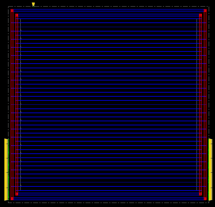
The layout itself is also an excellent source for additional analysis. The following figures illustrate some interesting aspects for a single design, the reference design at 500MHz (2ns clock).
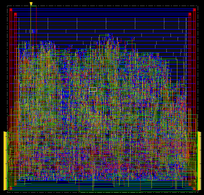
The full layout, showing 64 inputs coming in from the left, and producing 64 output bits on the right. Clock and reset ports are on top.
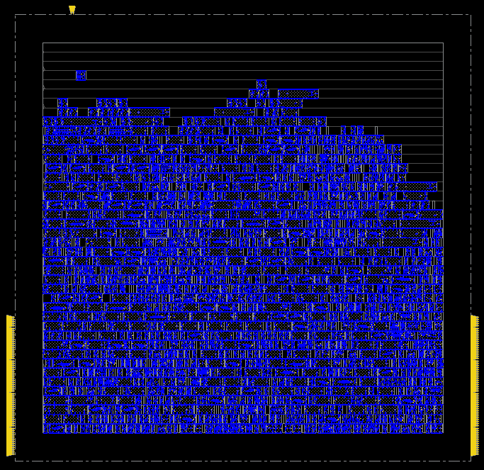
The standard cells only show that the design has a relatively high utilization; with an empty area at the top. This could be optimized as a modified aspect ratio, or a re-arranging of the I/O ports.
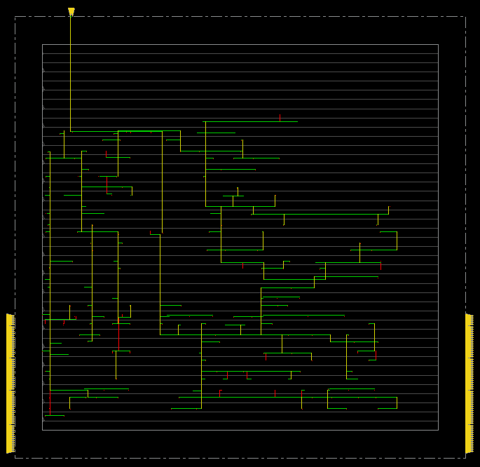
This shows the clock tree. At the leaf position of each branch is a flip-flop.
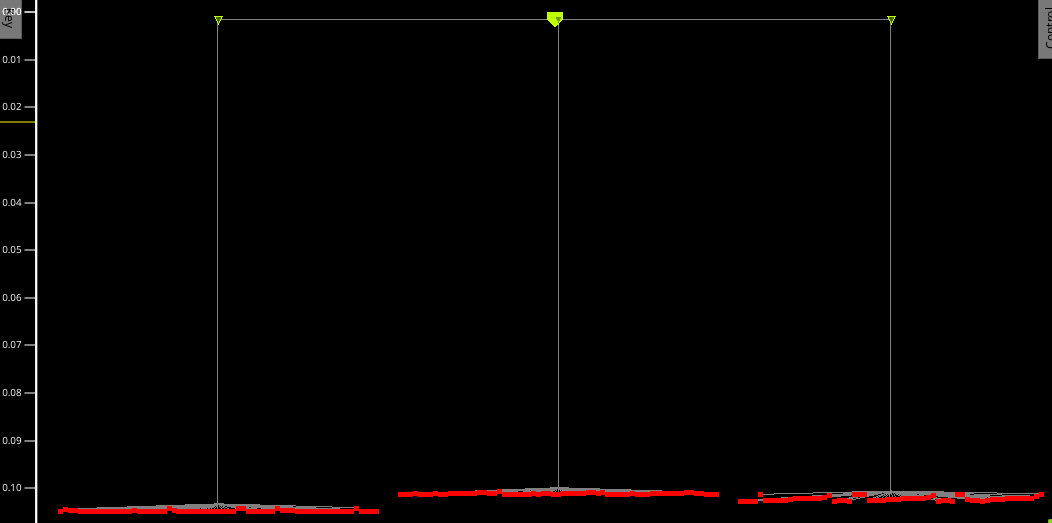
The clock tree is remarkably well balanced. The y axis in this graph shows clock delay, and the horizontal position enumerates flip-flops. Almost every flip-flop within a window of 0.05ns.
The layout uses a standard power grid, and no effort was made to create a mesh structure. This is very likely to cause problems for the standard cells in the middle of a row, who are too far apart from the power ring around the core. Hence, additional work is needed to design the power network of this layout. Separate analysis (signal integrity tools) can be used to determine of a power grid was well designed.
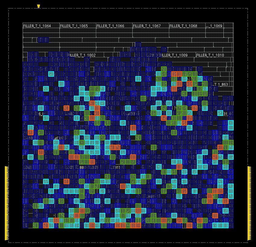
A pin density map shows which areas of the layout require most connections. A high pin density is correlated to routing congestion, as many wires need to converge in a single area of the chip.