Attention
This document was last updated Nov 25 24 at 21:59
Area-Time Tradeoff in a Hardware Multiplier
Important
The purpose of this lab is as follows.
Develop several configurations of a 16x16 (32-bit output) data multiplier. Each configuration represents a different trade-off between the number of clock cycles (latency) and the final area (gates, silicon area) needed to implement the multiplier.
The lab assignment covers the following tasks:
Writing RTL code for each multiplier configuration
Performing RTL simulation to verify the correctness of the design
Synthesizing the RTL to 45nm standard cells
Evaluate the time-area tradeoff by manipulating the synthesis constraints
Evaluate the impact of environment variables (process corners, temperature, voltage)
Evaluate the impact of the standard cell technology (130nm vs 45nm)
Collecting area, critical path and multiplier latency for each design and compare
Summarizing the results in a written report
Attention
The due date of this lab is 29 September
Introduction
The concept of area/time trade-off in hardware is fundamental. Area, in this lab, means the area used by the design on a silicon die. Time, in this lab, means latency (clock cycles * clock period) to complete a multiplication. Initially, will design the multiplier to operate at a 6 ns clock period, i.e. 166 MHz clock frequency.
Hardware implementations that run ‘at maximum speed’ are usually suboptimal. Only CPU designs, that have an infinite supply of instructions to execute, should run as fast as they can. In the majority of other applications, including embedded hardware designs, a hardware designer will try to balance area and time in such a manner that the design has the highest possible utilization.
In this lab you will design several multiplier designs. The outcome of the designs will be arranged in a plot as follows.
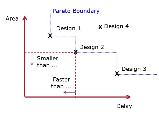
In this example, Design 1, Design 2 and Design 3 are all optimal in the sense that they give the smallest area for a given minimum delay constraint, or the smallest delay for a given maximum area constraint.
Design 4, however, is suboptimal to Design 2. Whenever the delay/area constraints are such that Design 4 could be chosen, Design 2 will give a smaller AND faster solution. One says that Design 1, Design 2 and Design 3 are pareto optimal for area and delay. Imagine Design 1, 2 and 3 each sitting at the lower left corner of a large rectange that reaches out to the upper left in the (Area, Delay) Space. All designs that are included inside of such a rectangle are suboptimal with respect to Design 1 or Design 2 or Design 3. Another way of looking at this space is that the three designs Design 1, Design 2 and Design 3 effectively define the design space of best hardware designs when(area, delay) trade-offs are considered. Design 1, 2 and 3 are pareto optimal and the staircase curve that connects these points is the pareto boundary. Of course, when additional criteria are introduced (power, need for special resources, design time, ..), then the trade-off becomes more difficult as it has to consider more dimensions. In this lab, we only care about area and delay.
Downloading Lab 1 and the Prerequisites
To start Lab 1, you need to download a repository as follows.
Important
Go to github classroom and instantiate your lab through the following link https://classroom.github.com/a/OGmAfnN2
After you have create the private repository, download it on your computer. The repository will include your account name. For example, in my case, Lab 1 would be cloned as follows after instantiation through github classroom:
git clone git@github.com:wpi-ece574-f24/lab-1-patrickschaumont.git
Note that the use for git@github.com requires you to set up a public key
on your GitHub account. If you don’t know how to do that, ask me in class.
Design Specifications
This section describes each of the four designs under consideration. All designs use the same testbench, which is discussed separately.
All of the multipliers will be implemented in 130nm Skywater standard cells and all multipliers must be able to achieve at least 100MHz clock frequency.
After download of the repository, you will find the following directory structure:
m1\constraints\      # in this directory, we place synthesis contraints (.sdc) for Design #1
m1\rtl\              # in this directory, we place RTL code for Design #1
m1\sim\              # in this directory, we simulate RTL code for Design #1
m1\syn\              # in this directory, we run synthesis for Design #1
Please note that this directory structure is only set up for a single design.
You can replicate additional multiplier directories from the m1 directory,
to accommodate Design #2, Design #3, and so forth. For example, cp -rp m1 m2.
Design #1: A single-cycle 16x16 bit multiplier
The baseline design is a 16x16 bit multiplier. The following design uses a single-cycle implementation. The input/output pins have the following meaning.
aandbare data inputsresultsreturns the 32-bit multipier outputstartis asserted when the input is validdoneis asserted when the result is valid.
In a single-cycle multiplier, start and done are trivivally related:
done is asserted a single cycle after start.
This particular implementation makes use of the multiply operation(*). The
RTL synthesis tool will expand this operator into individual combinational
gates.
Design #2: 16x16 bit multiplication by add-and-shift
The second, third and forth design have to be created by you. All designs implement the same 16x16 bit multiplication functionality, but their internal RTL design differs from design 1.
The second design has the same ports as the first design, but internally the multiplication is captured as add-and-shift.
The following example explains how this works. Assume that we have
to multiply two four-bit numbers, a = 1011 and b = 1001. We can
express this multiplication as follows.
a = 1011
b = 1001

a * b = 1011 * 1001
      = 1011 * (1 << 3  + 0 << 2 + 0 << 1 + 1 << 0)
      = 1*(1011 << 3) + 0*(1011 << 2) + 0*(1011 << 1) + 1*(1011)
      = (1011<<3) + (1011)
The multiplication of a and b creates partial products as shifted versions of a.
The multiplication is found by adding those partial products for which the corresponding bit in b is set.
In pseudocode, we would write this implementation as follows.
tmp = 0;
for i = 0 to 3
  if (b[i])
    tmp = tmp + a << i
result = tmp
Your implementation has to multiply using an add-shift expansion, but your multiplier has to finish in a single cycle. Effectively, your SystemVerilog code must be written in such a way that all partial products are added in a single clock cycle.
Design #3: 16x16 bit multiplication by add-and-shift, one add per cycle
In design variant 3, you will use the solution for design variant 2, and
modify it so that you add only a single partial product a << i to
tmp per clock cycle. A 16-bit operand therefore can take up to
16 clock cycles to be multiplied.
The benefit of doing only a single addition per cycle is that you can share the partial-product addition hardware over multiple clock cycles. Thus, the latency of Design 3 will be much higher than the latency of Design 1 and Design 2, but its area will smaller. This effect illustrates the area-time trade-off.
Design #4: 16x16 bit multiplication by add-and-shift, two add per cycle
In design variant 4, you will use the solution for design variant 2, and
modify it so that you can add two partial products a << i per clock
cycle. A 16-bit operand therefore can take up to 8 clock cycles to be
multiplied.
This intermediate design is a trade-off between Design 3 and Design 2: it uses less sharing than Design 3, but can complete a multiplication twice as fast. On the other hand, Design 4 is still smaller than Design 2, but it will have a longer latency.
Testbench
All multiplier designs share an identical testbench for functional verification. The testbench can be used for RTL simulation as well as gate level simulation. The testbench sets a 10ns clock period, and applies 1,024 random inputs to the multiplier. The testbench measures the latency of each multiplication (in clock cycles) and verifies the correctness of each result.
`timescale 1ns/1ps

module mymulttb;

   reg clk, reset;

   always #5 clk = ~clk;

   initial begin
      clk = 0;
      #5;
      reset = 1;
      #12;
      reset = 0;
   end

   logic [15:0] a, b;
   logic [31:0] r;
   int n;
   logic start;
   logic done;

   mymult1 DUT (
      .clk(clk),
      .reset(reset),
      .a(a),
      .b(b),
      .start(start),
      .result(r),
      .done(done)
   );

   int cycles, delta;
   initial cycles = 0;
   always @(posedge clk)
      cycles = cycles + 1;

   initial begin
      a = 16'b0;
      b = 16'b1;
      start = 0;

      $dumpfile("trace.vcd");
      $dumpvars(0, mymulttb);

      @(negedge reset);

      for (n = 0; n < 1024; n = n + 1) begin
         start = 1;
         delta = cycles;
         @(posedge done);
         delta = cycles - delta;

         $display("C %3d: a %x b %x m %x OK? %d", delta, a, b, r, (a * b) == r);

         start = 0;
         @(negedge done);

         a = $random;
         b = $random;

      end

      $finish;
   end

endmodule
The evaluation of each multplier (Design #1 through Design #4) goes through the following steps. You must repeat these steps for every design and maintain the results for your report. We will illustrate the steps with the intermediate outputs of a correct Design #1.
Part I: RTL Simulation
When you have specified your solution as rtl/mymult1.sv, you can then run
the RTL simulation in the rtl directory using make sim.
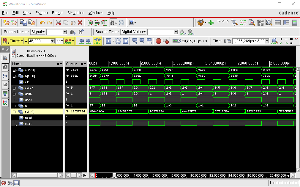
A correct output on the command line will look as follows:
$ make sim
xrun mymulttb.sv ../rtl/mymult1.sv -top mymulttb
TOOL:   xrun    22.09-s011: Started on Aug 22, 2023 at 17:51:58 EDT
xrun: 22.09-s011: (c) Copyright 1995-2023 Cadence Design Systems, Inc.
Loading snapshot worklib.mymulttb:sv .................... Done
xmsim: *W,DSEM2009: This SystemVerilog design is simulated as per IEEE 1800-2009 SystemVerilog simulation semantics. Use    -disable_sem2009 option for turning off SV 2009 simulation semantics.
xcelium> source /opt/cadence/XCELIUM2209/tools/xcelium/files/xmsimrc
xcelium> run
xmsim: *W,DVEXACC: some objects excluded from $dumpvars due to access restrictions, use +access+r on command line for access to    all objects.
            File: ./mymulttb.sv, line = 44, pos = 14
           Scope: mymulttb
            Time: 0 FS + 0

C   1: a 0000 b 0001 m 00000000 OK? 1
C   1: a 3524 b 5e81 m 139dff24 OK? 1
C   1: a d609 b 5663 m 4839cb7b OK? 1
C   1: a 7b0d b 998d m 49ce8b29 OK? 1
C   1: a 8465 b 5212 m 2a71a91a OK? 1
C   1: a e301 b cd0d m b5d3540d OK? 1
C   1: a f176 b cd3d m c195071e OK? 1
C   1: a 57ed b f78c m 5505c09c OK? 1
C   1: a e9f9 b 24c6 m 219bfa96 OK? 1
C   1: a 84c5 b d2aa m 6d41c4d2 OK? 1
C   1: a f7e5 b 7277 m 6ed73573 OK? 1
...
Alternately, you can also use make simgui which will run the Xcelium simulator
with GUI.
Don’t complete any synthesis tasks until you have a correctly working RTL simulation.
Part II: Synthesis on 45nm for a slow process corner
You will now run synthesis on the multiplier on the syn directory.
First, make sure you understand the synthesis script genus_script.tcl.
The script uses four environment variables to define synthesis conditions:
BASENAMEis a unique name that distinguish this synthesis setting from others. For example, if you change the synthesis constraints for timing, you can change theBASENAMEfor this run. This will change the file names used for intermediate output.CLOCKPERIODspecifies the clock period constraint in ns.TIMINGLIBspecifies the name of the standard cell timing view library to use in this synthesis.TIMINGPATHspecifies the path to the standard cell timing views of the standard cell library.
The Makefile shows how to specify the configuration for a synthesis run. For example, the default
sets a basename cds45_S_6 (Cadence 45nm, slow library, 6ns period), a 6ns clock, using the
library slow_vdd1v0_basicCells.lib stored in /opt/cadence/libraries/gsclib045_all_v4.7/gsclib045/timing/.
BASENAME=cds45_S_6 CLOCKPERIOD=6 TIMINGPATH=/opt/cadence/libraries/gsclib045_all_v4.7/gsclib045/timing/ TIMINGLIB=slow_vdd1v0_basicCells.lib genus -f genus_script.tcl
By adding additional targets in the makefile, you can specify synthesis with other clock constraints, base names, library paths and libraries. If your RTL simulation is operational, you can run the synthesis using make. The synthesis will take some time, but eventually produces results in an outputs directory and in a reports directory. Keep a close eye on any error message that you see, and fix the RTL if needed.
The output of the synthesis includes the following files.
outputs/cds45_S_6_constraints.sdc  # the constraints used in this synthesis run
outputs/cds45_S_6_delays.sdf       # the wire delays resulting from the synthesis (will be used in gate-level simulation)
outputs/cds45_S_6_netlist.v        # the resulting standard cell netlist
The reports of the synthesis describe the quality of the output.
reports/cds45_S_6_report_area.rpt   # shows cell count and active area (in sq micron)
reports/cds45_S_6_report_power.rpt  # shows a power estimation for this design
reports/cds45_S_6_report_qor.rpt    # shows a quality analysis (area and timing)
reports/cds45_S_6_report_timing.rpt # shows a static timing analysis result
For this lab, the most important output is the quality analysis file. Specifically, you have to record the following results:
cell count
active area
slack, which is defined as (clock_period - critical_path)
While we have not discussed timing analysis in detail yet, for now you can just assume that slack must always be positive for a correct design. When slack is negative, the design experiences a timing violation and the resulting netlist cannot be used at the specified clock period constraint.
Important
Analyze the pareto curve for each multiplier architecture under the 45nm slow process corner. You do this by completing multiple synthesis runs, each with a different clock period constraint. At a certain (long) clock period, you will find that area (cell count) no longer decreases. At a certain (short) clock period, you will find that the slack becomes negative. Your job is to find at least three points of the pareto curve. The two outer points must correspond to (a) the point at which the design area no longer decreases and (b) the point at which the slack becomes negative. Collect these points (eg in an excel sheet or on python matplotlib) and produce a pareto curve similar to the one shown above.
Part III: Synthesis on 45nm for a fast process corner, and for a 130nm slow process corner
Repeat Part II for two different library selections.
45nm fast process corner, high vdd:
TIMINGLIB=fast_vdd1v2_basicCells.libandTIMINGPATH=/opt/cadence/libraries/gsclib045_all_v4.7/gsclib045/timing/130nm slow process corner, high vdd, cold temperature:
TIMINGLIB=sky130_fd_sc_hd__ss_n40C_1v76.libandTIMINGPATH=/opt/skywater/libraries/sky130_fd_sc_hd/latest/timing/
Attention
Make sure to put some thought into how you can complete all these experiments efficiently, as they require many synthesis runs. By carefully coding a makefile, and possibly adding scripting to post-process the output files, you should be able to largely automate this task.
Final Analysis
After you have completed part I, II and III for each of the four multiplier architectures, you can now analyze the results. Produce pareto curves for each multiplier design and compare them:
What is the impact of each architecture on area?
What is the impact of each architecture on delay?
What is the impact of each architecture on the shape of the pareto curve?
Attention
Be careful when comparing pareto curves between different architectures. For example, a multiplier that uses 32 clock cycles to produce a result may be much smaller in area than a multiplier that needs only a single clock cycle. On the other hand, the delay of the 32-cycle multiplier equals 32 times the critical path of that multiplier, while the delay of the single-cycle multiplier equals its critical path. In other words, computing a result over multiple clock cycles proportionally increases the latency of the design, and that must be taken into account when drawing a pareto plot.
Preparing your report
In the final part of the design, you are going to analyze the design space exploration you have completed, and summarize the results in a report.
Include the following information in your report.
For each of the multiplier designs, include a listing of the SystemVerilog.
For each of the multiplier designs, include a pareto plot for the 45nm slow corner, the 45nm fast corner, and the 130nm slow corner.
Analyze the efficiency of each design and identify optimal designs. An optimal design is a design in the pareto plot for which the area * delay becomes minimal. Then, rank all of the designs according to that optimality criterium and produce a table with a ranked list:
Design |
Library |
Best area*delay |
Rank |
Design m1 |
45nm fast corner |
229847 |
1 |
Design m1 |
45nm slow corner |
280332 |
2 |
… |
… |
… |
… |
This table will contain 12 rows (4 designs and 3 libraries).
Attention
The following are important report requirements.
Use a typesetting tool such as latex or word. Do not submit handwritten scanned reports.
Use a screen capture tool to collect graphics such as layout information. Do not use your smartphone to take a picture from the screen.
Be clear and complete in your report. I am not looking for the correct solution; I am looking to understand your solution. Explain the steps that lead up to a result. The report does not have a minimum length nor a maximum length, as long as it is clear what you did and your answers to questions are complete.
Make sure to update, commit and push the results of your lab to your repository. You do not have to turn in anything on Canvas. All results will be communicated through your github repository.