Attention
This document was last updated Nov 25 24 at 21:59
Power Analysis and Optimization
Important
The purpose of this lecture is as follows.
To describe the components of power dissipation in hardware
To describe the factors that affect power dissipation in hardware
To describe design strategies that will optimize delay or energy of a design
to review the main ASIC design mechanisms to control power
To compare counter architectures from the power point of view
Important
The examples discussed in this lecture are available from https://github.com/wpi-ece574-f24/ex-counterpower
Attention
Power and Energy are among the most consequential factors in digital hardware design in the past three decades. Power is treated on equal footing with silicon area and delay, and the power profile of a design may make or break a product. The following are a few synoptic works on this sprawling topic.
Weste and Harris, “CMOS VLSI Design,” Chapter 5 or Lecture 7.
Rabaey, “Low Power Design Essentials”.
Chinnery and Keutzer, “Closing the Power Gap between ASIC and Custom”
Power and Energy Basics
Consider the following metrics which will play an important role in the power discussion:
Delay (s): A performance metric reflecting how long it takes to complete a task
Energy (J): An efficiency metric reflecting how much energy is required to complete a task
Power (W): An efficiency metric that normalizes the energy to the delay, reflecting the energy used per unit of time.
Energy.Delay (J.s): A combined performance and energy metric, used as a quality metric for a design style or orchitecture
Energy.Delay^2 (J.s^2): A combined performance and energy metric that increases the importance of delay over energy.
Most practical designs will care about both delay and energy. For example, delay minization without concern for the energy cost will yield very power-hungry solutions, while power minimization without concern for the performance will yield very slow solutions.
In CMOS designs, there are two major sources of power dissipation.
Dynamic Power: The charging and discharging of (parasitic) capacitors requires charge to be moved around in the chip. Every time the charge flows through a resistance, some energy is lost. In addition, every time a CMOS switch (with P and N transistor) switches, there is a short circuit current when both transistors are switching at the same time.
Static Power: Even when a CMOS circuit shows no activities, spurious currents remain because transistors are imperfect switches. Some analog components in digital circuits (e.g. sense amplifiers) require biasing currents, and these are also included with in the static power budget.
Dynamic Power
Let’s consider the energy being transferred as we charge (and discharge) a capacitor C. The setting is a CMOS inverter which drives an on-chip wire and several other gates. The wire and the combined inputs of those other gates can be modeled as a parastic load capacitor CL. As the inverter output makes a 0 to 1 transition, the p-channel transistor turns on and charges the capacitive load through the p-channel resistor Rp.
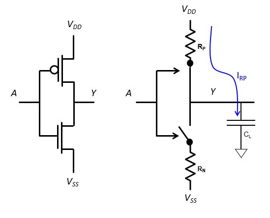
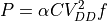
The total energy stored on the capacitor at the end of the transition is
The total energy dissipated as heat through the resistor  is equal to the energy stored on the capacitor. Supprisingly, it is independent of the value of the resistor.
Furthermore, during discharge, the energy stored on the capacitor flows to  and causes additional heat through dissipation in resistor
  .
.
This equation highlights the role of supply voltage as well as scaling in the power problem. Voltage has a quadratic dependency on power dissipated in CMOS logic. Hence, reducing the voltage by 0.7 will reduce the power by half. Furthermore, the capacitive load  is directly determined by the size of transitors, the length of wires, so that smaller circuits will consume less power. Thus, lowering the voltage, or reducing the feature size, contributed to reduced power consumption per gate. That does not mean that chips in smaller technologies consume less power: they also contain more gates. In fact, the power density, which is the power dissipated per unit of silicon area, is a major challenge in circuit scaling. As discussed in Lecture 1, the era of Dennard Scaling was ended in part because the power density for shrinking technologies was rising due to increased static power consumption.
The energy dissipated in the resistor depends also on the shape of the waveform. For a step response (i.e., charge as fast a possible), the dissipated energy equals the energy stored on the capacitor. But by slowing down the charging process, for example by using a slope instead of a step, or by using a current source instead of a voltage source, the dissipated energy is lower. Some circuit techniques have been developed to exploit this feature, although none of them has gained widespread industrial adoption so far.
This leads to the following formulation of dynamic power consumption of a CMOS
circuit with total capacitive load  .
.
where  is the switching rate and
  the probability that
a 0 to 1 transition will happen. This probability is often expressed as the
switching activity factor
the probability that
a 0 to 1 transition will happen. This probability is often expressed as the
switching activity factor  and we write
The activity factor is easy to derive for small and simple circuits. For example, assume a two-input AND gate with the following truth table.
A |
B |
Q |
|---|---|---|
0 |
0 |
0 |
1 |
0 |
0 |
0 |
1 |
0 |
1 |
1 |
1 |
If A and B have a random transition probability ( )
then the transition probability of the output is given by
)
then the transition probability of the output is given by
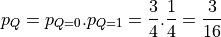
More generally, if the transition probabilities of the inputs are given by  and
and
 , then one can derive the following formulas.
AND |
|
XOR |
|

This may give the impression that one can derive the activity factor of a digital circuit through a symbolic computation. Unfortunately this is not the case.
One problem is that, in a large circuit, it becomes difficult to determine the precise transition probabilities of gate inputs. For example, in a reconvergent circuit (a circuit with multiple independent paths from a primary input to the fan-in of a gate), it’s no longer true that gate input probabilities are independent.
A second factor, which is possibly even harder to analyze, is that real digital circuits have state and feedback loops, so that a given input may encounter future copies of itself, which again breaks the independent distribution assumption. Therefore, in practice, power estimation is frequently done by simulation. One chooses a representative set of input test vectors, and then determines the average transition probability on each net.
The presence of reconvergent paths in a circuit leads to another problem as well in the form of dynamic hazards or glitches. Glitches are transient states that exist on a net while switching between states. Glitches are always parasitic, and should be kept to a minimum; glitch power is estimated to be around 20% of dynamic circuit power [Keutzer].
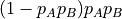
Short-circuit power is caused by the P and N transistor of a CMOS pair to be on simulateneously. There is a strong correlation between the transition delay of input and output on the one hand, and the short-circuit current on the other hand.
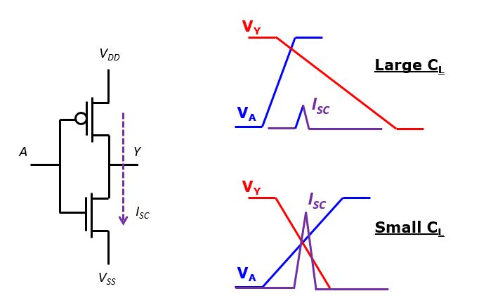
At large loading capacitance, the output transition will be slower than the input transition. This causes the inputs to have changed (P opening and N closing, for example) much faster than the output voltage has changed. Hence, the short-circuit current is small. At small loading capacitance, the output transition will be much faster, and can become faster than the input transition. In that case, the short-circuit current is substantially larger because the full output voltage comes across the open transistor while it is closing.
However, optimizing circuits so that input transitions are always fast, and output transitions are always slow, is not a good strategy to minimize the overall short-circuit current in a circuit. The reason is that a slow output may eventually drive another input, where it becomes a slow input and hence can drive up the short-circuit current of the driven gate. Therefore, a good implementation strategy is to equalize (make uniform) the transition delays over the complete circuit.
In practice, short-circuit power is modeled as a portion of the dynamic power consumption, because it occurs at every transition. Hence, one could model short-circuit power as an additional capacitive load that is added to the overall circuit.
Static Power
Transistors are never fully off. There’s always a small current, the leakage current. There is a variety of factors that contribute to the leakage current, all relating to transistor-circuit level effects. We will not consider these further.
However, there is an important observation to make on the connection between performance and leakage current. The leakage current depends on the threshold voltage, the voltage at which a transitor will switch from OFF to ON. At small  , the leakage current is higher. Unfortunately, a lower is beneficial for speed, as it allows a transistor to switch on sooner (faster). Hence, there is a trade-off between the performance of a circuit and the leakage current it creates.
The leakage power is approximated by product of the leakage current and the circuit voltage.
Overall Power
We can now derive the following expression for the power consumption of a CMOS circuit.

with
- the switching activity
- the load capacitance
 the short-circuit capacitance
 the voltage swing (
 for standard CMOS circuits)
- the clock frequency
 the leakage current
Modeling of Power and Energy
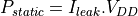
The gate-level models used for timing, namely Composite Current Source (CCS) and Non Linear Delay Models (NDLM), can be used for power estimation as well. As a reminder, the core idea of CCS and NDLM is to describe transitions with greater accuracy than just a direct 0 to 1 transition. In the case of NDLM, the transition delay of every transition is taken into account. In the case of CCS, multiple points are recorded for every transition to characterize the internal gate capacitance and behavior in even greater detail.
Such a gate-level model has access to the exact gate properties (type of gate, fan-in, fan-out, possibly voltage and temperature) as well as the behavior of the net transitions (transition delay or transition waveforms). Therefore it is possible to model not only timing, but also power.
There are three components to power with NDLM/CCS modeling. Unfortunately the terminology is a bit different from the dynamic and static power definitions we used earlier. Instead, NDLM/CCS uses the following three components.
Switching power is the power dissipated as a result of the output loading capacitance (fanout). The switching power directly depends on the output loading capacitance and on the transition delay on the input.
Internal power is the power dissipate as a result of cell-internal switching activities. The internal power directly depends on the output loading capacitance and on the transition delay on the input.
The leakage power is the leakage power caused by active components.
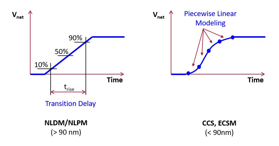
This more sophisticated model is necessary because cells from a cell library have a higher complexity than simple transistors. For example, the following example of a flip-flop contains 10 inverters (20 transistors). Modeling only the power due to transitions on the Q, QN outputs would ignore a significant portion of activity internally to the flip-flop.
Here is an example of an NDLM model for an inverter. Identify the leakage_power and internal_power sections. As with timing, the internal_power sections are based on lookup tables that are indexed/interpolated with output capacitance as well as input transition delay.
cell ("sky130_fd_sc_hd__inv_1") {
    leakage_power () {
        value : 0.0104575000;
        when : "A";
    }
    leakage_power () {
        value : 0.0001958000;
        when : "!A";
    }
    area : 3.7536000000;
    cell_footprint : "sky130_fd_sc_hd__inv";
    cell_leakage_power : 0.0053266820;
    driver_waveform_fall : "ramp";
    driver_waveform_rise : "ramp";
    pg_pin ("VGND") {
        pg_type : "primary_ground";
        related_bias_pin : "VPB";
        voltage_name : "VGND";
    }
    pg_pin ("VNB") {
        pg_type : "nwell";
        physical_connection : "device_layer";
        voltage_name : "VNB";
    }
    pg_pin ("VPB") {
        pg_type : "pwell";
        physical_connection : "device_layer";
        voltage_name : "VPB";
    }
    pg_pin ("VPWR") {
        pg_type : "primary_power";
        related_bias_pin : "VNB";
        voltage_name : "VPWR";
    }
    pin ("A") {
        capacitance : 0.0023020000;
        clock : "false";
        direction : "input";
        fall_capacitance : 0.0022140000;
        max_transition : 1.5000000000;
        related_ground_pin : "VGND";
        related_power_pin : "VPWR";
        rise_capacitance : 0.0023900000;
    }
    pin ("Y") {
        direction : "output";
        function : "(!A)";
        internal_power () {
            fall_power ("power_outputs_1") {
                index_1("0.0100000000, 0.0230505800, 0.0531329300, 0.1224745000, 0.2823108000, 0.6507428000, 1.5000000000");
                index_2("0.0005000000, 0.0013351650, 0.0035653330, 0.0095206180, 0.0254232000, 0.0678883500, 0.1812843000");
                values("-0.0020153000, -0.0032337000, -0.0066826000, -0.0162151000, -0.0419235000, -0.1106943000, -0.2943854000", \
                    "-0.0022916000, -0.0034843000, -0.0068641000, -0.0163126000, -0.0419618000, -0.1107056000, -0.2943928000", \
                    "-0.0025042000, -0.0037542000, -0.0071223000, -0.0164928000, -0.0420580000, -0.1107451000, -0.2944136000", \
                    "-0.0024712000, -0.0037581000, -0.0073060000, -0.0167240000, -0.0422169000, -0.1107988000, -0.2944345000", \
                    "-0.0020559000, -0.0034396000, -0.0072092000, -0.0167699000, -0.0423050000, -0.1109175000, -0.2944570000", \
                    "-0.0010220000, -0.0025801000, -0.0064007000, -0.0161275000, -0.0421627000, -0.1109094000, -0.2945079000", \
                    "0.0018716000, 0.0002414000, -0.0040818000, -0.0145818000, -0.0408514000, -0.1101701000, -0.2941599000");
            }
            related_pin : "A";
            rise_power ("power_outputs_1") {
                index_1("0.0100000000, 0.0230505800, 0.0531329300, 0.1224745000, 0.2823108000, 0.6507428000, 1.5000000000");
                index_2("0.0005000000, 0.0013351650, 0.0035653330, 0.0095206180, 0.0254232000, 0.0678883500, 0.1812843000");
                values("0.0077341000, 0.0092285000, 0.0130076000, 0.0228389000, 0.0486009000, 0.1169039000, 0.2980101000", \
                    "0.0075137000, 0.0089827000, 0.0128048000, 0.0225722000, 0.0483903000, 0.1157698000, 0.2983583000", \
                    "0.0074664000, 0.0088070000, 0.0125411000, 0.0222793000, 0.0479465000, 0.1162597000, 0.2988481000", \
                    "0.0074628000, 0.0088101000, 0.0124018000, 0.0220691000, 0.0478142000, 0.1160948000, 0.2978862000", \
                    "0.0085703000, 0.0097756000, 0.0131398000, 0.0225755000, 0.0477140000, 0.1159043000, 0.2976869000", \
                    "0.0117396000, 0.0133470000, 0.0162555000, 0.0258334000, 0.0499281000, 0.1175191000, 0.2963656000");
            }
        }
        max_capacitance : 0.1812840000;
        max_transition : 1.4983500000;
        power_down_function : "(!VPWR + VGND)";
        related_ground_pin : "VGND";
        related_power_pin : "VPWR";
        timing () {
            cell_fall ("del_1_7_7") {
                index_1("0.0100000000, 0.0230506000, 0.0531329000, 0.1224740000, 0.2823110000, 0.6507430000, 1.5000000000");
                index_2("0.0005000000, 0.0013351700, 0.0035653300, 0.0095206200, 0.0254232000, 0.0678883000, 0.1812840000");
                values("0.0143656000, 0.0174314000, 0.0252454000, 0.0454996000, 0.0982781000, 0.2396302000, 0.6168033000", \
                    "0.0188850000, 0.0219910000, 0.0299354000, 0.0501644000, 0.1030737000, 0.2443058000, 0.6211737000", \
                    "0.0258174000, 0.0306806000, 0.0410519000, 0.0615784000, 0.1142486000, 0.2560606000, 0.6330331000", \
                    "0.0343699000, 0.0422631000, 0.0579953000, 0.0872580000, 0.1417882000, 0.2823734000, 0.6608606000", \
                    "0.0429306000, 0.0551406000, 0.0803595000, 0.1251743000, 0.2024078000, 0.3451943000, 0.7237922000", \
                    "0.0467306000, 0.0653220000, 0.1038849000, 0.1743242000, 0.2939730000, 0.4885973000, 0.8661273000", \
                    "0.0317479000, 0.0590882000, 0.1188517000, 0.2277923000, 0.4124719000, 0.7155372000, 1.2016104000");
            }
            cell_rise ("del_1_7_7") {
                index_1("0.0100000000, 0.0230506000, 0.0531329000, 0.1224740000, 0.2823110000, 0.6507430000, 1.5000000000");
                index_2("0.0005000000, 0.0013351700, 0.0035653300, 0.0095206200, 0.0254232000, 0.0678883000, 0.1812840000");
                values("0.0203433000, 0.0255806000, 0.0388749000, 0.0728467000, 0.1628902000, 0.4016502000, 1.0383745000", \
                    "0.0255253000, 0.0306373000, 0.0439316000, 0.0783240000, 0.1679452000, 0.4092315000, 1.0428830000", \
                    "0.0373555000, 0.0435741000, 0.0566328000, 0.0903158000, 0.1807958000, 0.4194971000, 1.0619717000", \
                    "0.0547083000, 0.0647747000, 0.0847049000, 0.1211221000, 0.2113354000, 0.4503315000, 1.0860455000", \
                    "0.0801236000, 0.0963068000, 0.1281064000, 0.1863159000, 0.2799442000, 0.5189765000, 1.1578426000", \
                    "0.1184431000, 0.1426164000, 0.1928426000, 0.2835618000, 0.4327621000, 0.6847846000, 1.3109622000", \
                    "0.1833476000, 0.2165725000, 0.2904738000, 0.4311227000, 0.6701159000, 1.0433531000, 1.6968695000");
            }
            fall_transition ("del_1_7_7") {
                index_1("0.0100000000, 0.0230506000, 0.0531329000, 0.1224740000, 0.2823110000, 0.6507430000, 1.5000000000");
                index_2("0.0005000000, 0.0013351700, 0.0035653300, 0.0095206200, 0.0254232000, 0.0678883000, 0.1812840000");
                values("0.0078064000, 0.0114862000, 0.0214097000, 0.0477227000, 0.1186008000, 0.3072657000, 0.8034127000", \
                    "0.0090602000, 0.0121604000, 0.0214004000, 0.0478255000, 0.1185653000, 0.3042409000, 0.8075141000", \
                    "0.0149965000, 0.0184620000, 0.0253538000, 0.0485230000, 0.1183136000, 0.3050132000, 0.8077053000", \
                    "0.0252848000, 0.0304682000, 0.0408323000, 0.0598601000, 0.1207760000, 0.3047933000, 0.8058169000", \
                    "0.0433758000, 0.0513324000, 0.0671383000, 0.0963828000, 0.1477217000, 0.3113176000, 0.8041146000", \
                    "0.0756267000, 0.0875932000, 0.1123155000, 0.1572394000, 0.2319551000, 0.3682797000, 0.8125686000", \
                    "0.1370231000, 0.1548396000, 0.1933634000, 0.2609415000, 0.3750985000, 0.5666359000, 0.9242953000");
            }
            related_pin : "A";
            rise_transition ("del_1_7_7") {
                index_1("0.0100000000, 0.0230506000, 0.0531329000, 0.1224740000, 0.2823110000, 0.6507430000, 1.5000000000");
                index_2("0.0005000000, 0.0013351700, 0.0035653300, 0.0095206200, 0.0254232000, 0.0678883000, 0.1812840000");
                values("0.0145424000, 0.0213070000, 0.0395425000, 0.0876798000, 0.2171014000, 0.5586131000, 1.4687663000", \
                    "0.0146713000, 0.0213043000, 0.0393699000, 0.0877615000, 0.2159054000, 0.5600529000, 1.4722740000", \
                    "0.0211790000, 0.0256255000, 0.0404175000, 0.0878470000, 0.2163130000, 0.5577243000, 1.4753007000", \
                    "0.0345207000, 0.0410610000, 0.0542730000, 0.0916769000, 0.2161580000, 0.5606987000, 1.4678798000", \
                    "0.0568227000, 0.0674569000, 0.0881982000, 0.1265939000, 0.2258740000, 0.5582781000, 1.4769377000", \
                    "0.0919248000, 0.1090963000, 0.1442140000, 0.2030622000, 0.2988102000, 0.5742777000, 1.4743026000", \
                    "0.1521643000, 0.1785044000, 0.2319170000, 0.3280231000, 0.4842423000, 0.7386280000, 1.4983498000");
            }
            timing_sense : "negative_unate";
            timing_type : "combinational";
        }
    }
}
Vector-driven versus Vector-less power estimation
Some tools, such as static timing analyzers, allow you to make a quick estimate of dynamic and static power consumption, based on basic transition probabilities. The transition probabilities are just that, they are guesses on circuit activity rather than the result of actual simulation. The power numbers from such estimates are a useful quick estimate.
As an example, consider the following 8-bit counter module.
module bcounter8(
                input wire         clk,
                input wire         reset,
                output wire [7:0] q);

   reg [7:0]                       areg;
   reg [7:0]                       areg_next;

   always @(posedge clk, posedge reset)
     if (reset)
       areg  <= 8'b0;
     else
       areg  <= areg_next;

   always @(*)
     areg_next = areg + 8'b1;

   assign q = areg;

endmodule
This counter module results in 32 cells, including 8 flip-flops, and a collection of combinational cells (total area 355.34 sqmu). The power estimate shows that most power dissipation is internal.
Group                  Internal  Switching    Leakage      Total
                          Power      Power      Power      Power (Watts)
----------------------------------------------------------------
Sequential             3.28e-05   1.97e-06   2.55e-11   3.47e-05  91.6%
Combinational          1.87e-06   1.34e-06   4.22e-11   3.20e-06   8.4%
Macro                  0.00e+00   0.00e+00   0.00e+00   0.00e+00   0.0%
Pad                    0.00e+00   0.00e+00   0.00e+00   0.00e+00   0.0%
----------------------------------------------------------------
Total                  3.46e-05   3.30e-06   6.77e-11   3.80e-05 100.0%
                          91.3%       8.7%       0.0%
If we increase the counter module to a 32-bit output, its size increases to 150 cells (more than 4.68x) and the area to 1526 sqmu (4.29x). The power dissipation increases to 146 microWatt (3.84x). Its easy to see that this is probably too pessimistic, because the activity of the higher-order bits in a sequential counter is significantly lower.
Group                  Internal  Switching    Leakage      Total
                          Power      Power      Power      Power (Watts)
----------------------------------------------------------------
Sequential             1.30e-04   5.56e-06   1.02e-10   1.36e-04  92.9%
Combinational          5.69e-06   4.63e-06   1.64e-10   1.03e-05   7.1%
Macro                  0.00e+00   0.00e+00   0.00e+00   0.00e+00   0.0%
Pad                    0.00e+00   0.00e+00   0.00e+00   0.00e+00   0.0%
----------------------------------------------------------------
Total                  1.36e-04   1.02e-05   2.66e-10   1.46e-04 100.0%
                          93.0%       7.0%       0.0%
Accurate power estimation therefore makes use of vector stimuli, which reflect actual transitions (See handson).
Design Philosophy: Performance vs Power
Because of the high importance of power and energy in modern digital design, it is relevant to consider how to optimize a design in the design space power-area-performance. We have already discussed the trade-off between area and delay, and we are aware of design techniques such as pipelining, unfolding, multiplexing and bit-serializing to navigate the area/delay space.
But we cannot ignore power. In high-performance design, power is limited by the thermal limits of the implementation. For example, high-performance processors are no longer scaled in frequency/voltage (see lecture 1). The unrelented scaling for performance resulted in a chip that was infeasible from a power consumption (thermal) perspective.
The design philosophy of maximizing the clock frequency at all cost therefore is replaced a one in which the acceptable latency of the design is used to relax the clock, and in return lower the power consumption. In some fields (such as real-time embedded systems), designing systems as fast as needed rather than as fast as possible is very natural. In classic performance-oriented fields such as processos, this shift may be less obvious.
But even when performance is still important, we can still limit the clock frequency increase by building a design with more parallellism. This way, you can see how area plays a role in the trade-off between performance and power. Modern successful designs are not high-frequency, but rather efficient and specialized. The System-on-Chip architecture, which extends a small but flexible processor with multiple specialized hardware accelerators/peripherals, is an example of the idea that high performance in a specific domain can be coupled to low power.
Low-power Design Flow
There are a wealth of techniques that support power optimization of a design. In the following discussion, we will emphasize circuit-level techniques and concepts. However, for a complete treatment of power optimization, you should take a look at the Low Power Design Essentials book by Rabbaey.
Power optimization works by impacting the factors that contribute to the power consumption. As we derived earlier:
Reducing Activity
An obvious handle to power reduction is to reduce activity, i.e. to reduce the switching factor  . Some of the techniques to support this optimization include the following.
Clock gating: The clock signal is the biggest and most active signal in a synchronous digital design. Clock gating implies that the clock signal is turned off when the block is not active. Clock gating only affects dynamic power consumption.
Reducing glitches: Glitches are useless transitions caused by variations in the propagation delay of circuits. Glitch removal requires balancing of delay paths on logic networks – something that requires manual design.
Demultiplexing: Hardware multiplexing causes extra transitions by definition, because the logic is switched between multiple independent data bits. The epitome of a multiplexed circuit is probably the bit-serial design, which causes every data bit of an n-bit word to be passed through n registers in the serialization process. Word-parallel designs, that don’t multiplex hardware, can reduce these extra transitions. Of course, when hardware is no longer multiplexed, the design will grow in size. Eventually, the advantage of power savings will get lost.
Encoding: Data encoding techniques can mimize additional transitions as well. For example, one-hot encoding (indicating a 1-out-of-n choice with n bits) will have only two transitions code change; gray-code encoding will have only two transitions per code change when the code change is incremental. Considerations for encoding are application dependent, and design automation will only handle specialized cases such as FSM state encoding.
Reducing
Gate sizing: The capacitive load driven by a gate is directly influenced by the types of gate driven: a higher load means a slower gate. Hence, by resizing cells (i.e. replacing a cell with an equivalent one of larger or smaller drive strength), we can locally adjust the performance of a circuit. The performance trade-off will benefit power, as well. A slower gate comes with slower transition times, reducing the power consumed by the gate. Design automation tools, who are aware of the available positive slack at each gate, can therefore try to adjust the drive strength of each gate to balance performance and power. The net result is that the variation in slack over the entire circuit is reduced, while at the same time the performance of the entire circuit overall is made more uniform.
Reducing Short-circuit Power
Short-circuit Power is minimized by making sure no excessive transition times exist on each not. Also, short-circuit power can be reduced by using high- transistors.
Power Gating
Multi-voltage Domains: The most obvious transformation to reduce voltage swing is the lower the operating voltage. In practical low-power design, multiple voltages will exist in the chip to accommodate for the performance need of every major module. The introduction of multiple voltage domains can only be done when the standard cell library is capable of supporting multiple voltages. Indeed, additional specialized cells are needed to support the use of multiple voltages.
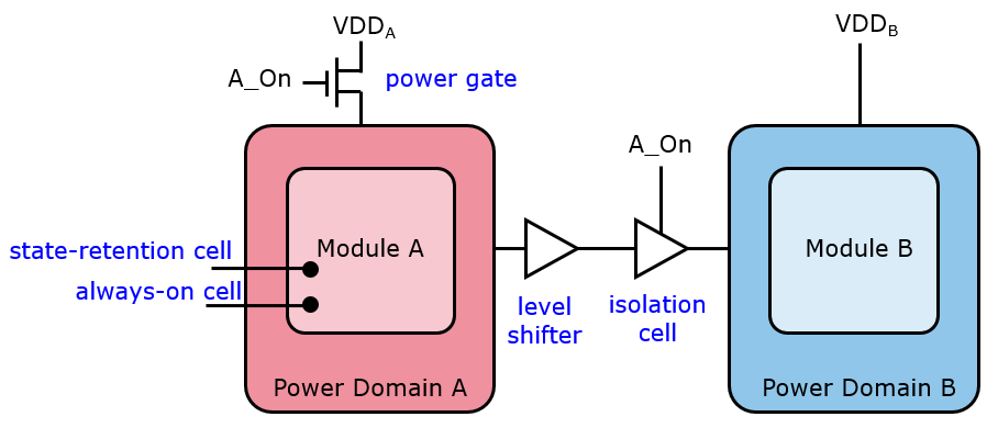
Assume a chip with two power domains, A and B. Both power domains use a different operating voltage, optimized towards the power/performance trade-off for each domain. Power domain A is controlled through individual power gates which can turn on or off the voltage for that domain. To communicate between the power domains, level shifter gates are needed to translate logic high/low voltage levels from one domain to the other. Furthermore, isolation cells are used to isolate domain B from the driving domain A, when A is turned off. The isolation cells prevent floating inputs on the B domain, which can cause spurious transitions in the B domain, and which inject unknown values in B. When A is off, additional cells may be used to help A recover from the shutoff. State retention cells are special flip-flop cells which accept an always-on voltage which will retain their state when the main voltage is turned off. Always-on buffers are buffers that stay on when the main voltage is turned off; they help control the retention-control pins on the state retention cells.
Multi-voltage domains are essential in low-power applications that need to shutdown a major part of a chip. Once a power domain is shut off, both the dynamic power and the static power dissipation on that domain are zero.
Flexible Voltage/Frequency
Control of the operating voltage as well as the frequency are important turning knobs in the control of dynamic and static power consumption. The operating voltage affects dynamic as well as static power, while the frequency affects the dynamic power.
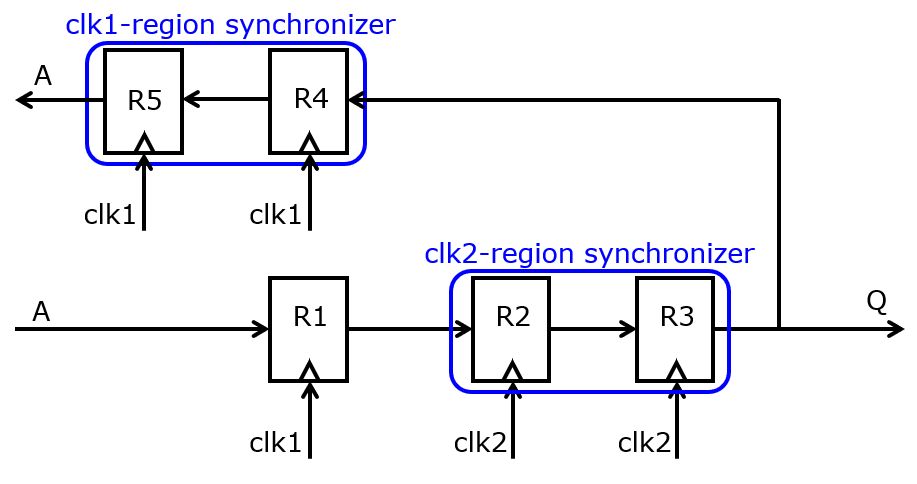
Chips with multiple frequency domains can be made just like chips with multiple voltage (power) domains. When moving from one frequency domain to the next, a separate synchronizer circuit must be introduced to avoid metastability. In the following example, a transition from a fast clock domain clk1 to a slow clock domain clk2 is demonstrated. Two back-to-back registers within a single clock domain is used as a synchronized; such a setup prevents metastability from the front-end flip flop into the target clock domain. To ensure that the slow clock domain clk2 has successfully read the value Q, the bit is send back to the fast clock domain to a clk1 synchronizer. The fast clock domain clk1 is only allowed to remove input bit A when it is able to see that the bit was properly received in clock domain clk2.
Reducing
Because static power consumption is a dominant factor inadvanced technology nodes, a range of techniques is used to minimize its contribution.
High-Vt transistors: A library with cells with a high threshold voltage will show less leakage than the standard-threshold equivalent. The disadvantage of such a library is that these cells are slower than their standard counterparts.
Substrate biasing: By driving the subtrate voltage of a cell, its leakage can be reduced as well. Substrate biasing requires cells with two additional voltage-bias inputs, one for the p-MOS transistors in the cell, and one for the n-MOS transistors.
It is clear that there is a rich collection of techniques available to tackle static and dynamic power consumption of CMOS logic. Two crucial elements to apply such power-reduction techniques are (a) thoroughly understand the application and its needs, and (b) use design automation support where possible - such as with gate sizing, power domain design, and clock gating.
Power Estimation in Joules
Please refer to Canvas for links to relevant background reading