Attention
This document was last updated Nov 25 24 at 21:59
System On Chip
Important
The purpose of this lecture is as follows.
To describe the typical architecture of a system-on-chip (SoC)
To introduce the IBEX RISC-V 32-bit processor as a ceontral control element in SoC
To introduce the relevant abstraction layers of design in SoC
To discuss memory-mapped coprocessing as a mechanism to integrate custom-hardware in SoC
To experiment with memory-mapping in the context of IBEX
Attention
The following references are relevant background to this lecture.
Schaumont, “System on Chip,” Chapter in A Practical Introduction to Hardware Software Codesign, Springer. https://link.springer.com/chapter/10.1007/978-1-4614-3737-6_8.
Pasquale Davide Schiavone, Francesco Conti, Davide Rossi, Michael Gautschi, Antonio Pullini, Eric Flamand, Luca Benini, “Slow and steady wins the race? A comparison of ultra-low-power RISC-V cores for Internet-of-Things applications,” PATMOS 2017: 1-8. https://doi.org/10.1109/PATMOS.2017.8106976
RISCV Consortium, RISC-V Technical Specifications.
The System On Chip Architecture
In many ways, modern hardware design is about finding the right tradeoff between specialization and flexibility in the design. A higher level of specialization results in a higher of performance of the implementation and a better energy efficiency. On the other hand, high levels of specialization have limited use. When chips are expensive to build, it’s better to make sure that a single chip can be used for multiple purposes.
The system-on-chip is a system architecture that is fundamentally built around this trade-off of specialization and general-purpose design. The core idea is to combine a programmable element, typically a small processor, with several dedicated hardware modules that perform specialized operations. The general-purpose functionality is achieved by software running on the processor, while the specialized functionality is achieved by the hardware modules integrated around the processor.
Micro-controllers have followed the system-on-chip architecture for many years, because of their need to combine dedicated input/output peripherals with software functionality. For example, an motor speed control application may require a high-resolution timer module with pulse-width-modulation output, while an automotive application may need one or more CAN (Controller Area Network) interfaces for communication with sensor units distributed over a car’s body. Different application domains can thus be translated into different microcontroller families which each provide a mix of peripherals that optimized to the application domain.
The following figure (taken from a TI MSP-430 User Guide) is a blueprint of a typical microcontroller with an SoC architecture. The left side of the figure shows the processor along with on-chip storage for data and code. The right side of the figure shows a number of peripherals, all attached to the same bus as the processor memories. From the hardware point-of-view, the interface between the peripherals and the processor looks the same as the interface between the memories and the processor. From the software point-of-view, the peripherals appear as memory locations to the processor. Software can read and write into these memory locations to exchange data with the hardware peripherals. This concept of memory-mapped hardware is central to the system-on-chip architecture. It supports the integration of dedicated hardware into a larger system, while it is backward compatible with the software development tools used by the processor.

The memory-mapped interface is extremely scalable: as many peripherals can be integrated as needed. Of course, these peripherals must each respond to different locations into the memory space of the processor. However, the memory-mapped interface is not a panacea, and the memory-bus can quickly become a bottleneck because it is shared between all peripherals and the processor memory. Hence, memory-mapped interfaces are not suited when high-speed communication between the peripheral and the software (or between peripherals among themselves) is needed. However, that disadvantage is easily outweighed by the advantage of an easy-to-use, extensible interface for dedicated hardware modules. The chapter on System on Chip under the reading materials summarized the most important characteristics of the system-on-chip architecture.
In this course, we will use the system-on-chip architecture as a baseline for hardware designs. We will use a RISC-V processor as the central processor, and extend it with memory-mapped peripherals. We will also study other mechanisms of customization, such as modifying the RISC-V processor with new instructions. However, this is not a course on System-on-Chip design, and the focus will be squarely on the hardware design aspects of SoC. By studying hardware design in the context of SoC architectures, we experience the constraint of a real hardware interface, and a testing environment corresponding to a common integration scenario.
IBEX, a 32-bit RISC-V processor
IBEX is a processor that was initially developed under the name zero_riscy, and is now maintained by lowRISC as an open-source project. IBEX has been used by a number of highly visible open-source projects such as OpenTitan, a root of trust for modern compute infrastructure.

IBEX splits the execution of each instruction in three stages - fetch, decode/execute, and writeback. IBEX supports two configurations of the base RISC-V instruction set. These instruction sets are focused on embedded and low-power operation.
Name |
Description |
|---|---|
RV32I |
32-bit Base Integer Instrution Set |
RV32E |
32-bit Embedded w 16-bit Registers |
Several extensions can be added to the base instruction sets. When an IBEX core is configured, these extension identifiers are appended to define the overall instruction set of the core. For example, RV32IMC means a core with a 32-bit base instruction set, integer multiplication and division, and compressed instruction support.
Name |
Extension |
|---|---|
C |
Extension for compressed instructions (always on) |
M |
Integer Multiplication/Division |
B |
Bit Manipulation |
ZICSR |
Control/Status Reg Manipulation (always on) |
Attention
The main repository for the IBEX core is https://github.com/lowRISC/ibex. This repository contains the hardware description as well as the configuration scripts to create cores with various capabilities. The documentation website is an indispensable guide to configure and use the core.
Abstraction Levels in SoC Design
In SoC design, it is common to reason about a design at multiple levels of abstraction. Hardware designers commonly use RTL (register-transfer level) and gate-level abstractions. However, when a programmable processor enters the picture, RTL is too low-level, and incapable of distinguishing the fixed part (hardware and processor) from the flexible part (software running on the processor). Therefore, additional, higher-level abstractions are used. In the following, we assume that the software running on the SoC processor is running in bare-metal mode, i.e., there is no operating system nor virtualization involved, and ‘software’ means a single-threaded executive.
We define four abstraction levels (Application, Instruction-set, RTL and Gate-level). Each of these abstraction levels is naturally captured by a model for time, for software and for hardware, as in the following table.
Level |
Time Model |
Software Model |
Hardware Model |
Application |
Transaction |
ABI |
HAL |
Instruction-set |
Instructions |
ISA |
Memory Ops, Custom-Ins Ops |
RTL |
Clock Cycle |
Opcodes & Image |
Register Transfers |
Gate-level |
Event |
Bits |
Gates + Macro’s |
We will work through the table from the lowest abstraction level to the highest. The Level column shows the name of each abstraction level. The Time Model column shows the smallest time step in behavior that is typically considered. The Software Model shows the common abstraction model used to define software. In essence, the software model is the interface under which the lower abstraction levels are hidden. The Hardware Model is the common abstraction model used to define hardware. As with software, the hardware model is expressed in terms of interfaces that hide low-level details.
The Gate-level is the lowest abstraction level defined in the table. Software and hardware are logically indistinguishable, although at this level you can map hardware into structural elements (a netlist of gates and dedicated macro’s), and map software into bits occupying memory modules and/or registers. The gate-level is very detailed, and captures all activities in the chip as events: (time, value) tuples. The Gate-level is a detailed representation that helps one to understand the physical characteristics of the chip, such as its power consumption, maximum clock frequency, and silicon area. But it is exceedingly difficult to understand the chip’s activities at the macroscopic level.
The Register-transfer level (RTL) is a crucial stepping stone between a chip’s high-level model that emphasizes functionality, and the gate-level model that emphasizes physical realization. In an RTL model, all registers in the design are accurately captured, and their update is captured per clock cycle. However, the operations between registers are abtracted out into functional expressions. One of the great achievements of modern EDA is that design automation tools are able to make the transition from the RTL to the gate-level automatically through logic synthesis. Yet, RTL is much easier to understand to a hardware designer. RTL also recognized the association between bits into words. This allows us to think of software models as a sequence of opcodes. RTL is a natural modeling level of hardware designers, but requires a bit of effort in understanding from the software point of view.
The Instruction-Set level captures the behavior of the SoC in terms of instructions of the target processor. The smallest activity in the SoC is the execution of a single instruction, even if this instruction extends over multiple clock cycles. At this level, software is defined by the Instruction-set Architecture (ISA) of the processor. Also, at this level, hardware starts to disappear behind these abstractions. For example, ISA hides the low-level implementation details of the SoC processor, while the SoC peripherals and hardware modules are abstracted into memory locations and (in some cases) specialized instructions on the processor. The instruction-set level is naturally useful to the firmware designer. Because of the pronounced abstraction of low-level details, instruction-level simulation tends to be very fast (with simulation speeds running into KHz to MHz on typical workstations). Yet, the reduced visibility of hardware details at this level means that it is hard to capture hardware bugs.
The Application level is the highest abstraction level we’ll consider at this moment. At this point, both the hardware and the software are abstracted into an interface that emphasized functionality. Software uses an Application Binary Interface (ABI) to abstract the major functional details of the SoC processor (such as the stack, the interrupt model, the memory organization, and so on). Hardware uses the Hardware Abstraction Layer (HAL) which replaces the interaction with dedicated hardware modules by a simple funtion call. The large granularity of modeling usually also affects the time granularity. Application-level models emphasize transaction-level statistics such as number of bus operations, or the number of bytes transferred in one HAL call. Application-level models are crucial for system designers to create the SoC’s blueprint. But they cannot reveal detailed implementation metrics such as the area, gate-count or power of a design.
The table above is not an exhaustive list of abstraction levels. An important abstraction level below that of gate-level is the layout, which is a purely structural description. Likewise, there are additional levels above the application level, where hardware and software merge into a purely functional model of computation. In this course on Advanced Digital Systems Design, our emphasis will be on the RTL and below (Gate, Layout). However, to understand the SoC’s design and operation, the instruction-set level plays an important role as well.
Important
Our objective in the project will be to design hardware accelerator modules for an IBEX based SoC. That is the primary motivation for studying SoC design in this lecture.
A corollary of the above observations on abstraction level, is that it is meaningful to consider multiple simulation-levels for a system on chip. Instruction-level simulation, for example, would be useful to develop and test software (firmware) for the SoC once the hardware is more or less fixed. Cycle-accurate simulation (at the RTL level) would be useful to efficiently co-simulate hardware and software, but without consideration about the detailed timing-dependent hardware-level effects. Cycle-accurate simulation will not be as quick as instruction-level simulation, but still fast enough to cover, say, a few million clock cycles in an hour. Gate-level simulation, with full timing accuracy, would help understand the low-level effects on the hardware platform, such as race conditions and timing faults. But realistically, a gate-level simulation can cover only a few thousand clock cycles in an hour, and so this level is no longer suitable for SoC firmware development.
While we use IBEX, we will similarly use multiple simulators to study the design at each abstraction level. IBEX supports Verilator, a cycle-accurate HDL simulator that efficiently runs firmware applications on IBEX. We will eventually also use XCelium as a gate-level simulator for IBEX-based chips. But the initial experiments will be based on Verilator.
IBEX Instructions
When evaluating an embedded SoC, we frequently run into assembly programs for the embedded processor. Even if we write C and use a C compiler, the output of the compiler will often be evaluated at the assembly level in order to answer precise questions regarding the performance of the design. For this reason, we also consider RISC-V assembly coding.
The standard RISC-V processor has 32 32-bit registers. Their generic name starts with an X: X0 to X31. However, assemblers will often use a naming that is compatible with the standard C ABI for RISC-V. The following table lists the register names and their primary purpose.
Reg Name |
Symbolic Name |
Description |
Saved by |
|---|---|---|---|
X0 |
zero |
Always zero |
|
X1 |
ra |
Returns Address |
Caller |
X2 |
sp |
Stack Pointer |
Callee |
X3 |
gp |
Global Pointer |
|
X4 |
tp |
Thread Pointer |
|
X5-7 |
t0-2 |
Temporary |
Caller |
X8 |
s0/fp |
Frame Pointer |
Callee |
X9 |
s1 |
Saved Register |
Callee |
X10-17 |
a0-7 |
Function Argument |
Caller |
X18-27 |
s2-11 |
Saved Register |
Callee |
X28-31 |
t3-6 |
Temporary |
Caller |
Assembly code for an embedded processor such as IBEX is typically
created as a byproduct of compiling a firmware application. A compiler that
produces code for a processor different from the processor that is used
for running the compiler is a cross-compiler. To create IBEX programs, we will
use a cross-compiler for C programs. On the class design server, the
cross-compiler is installed under /opt/lowrisc-toolchain-rv32imcb-...
The dots hold the compiler release date. To use the compiler, you’d also set
the path to the compiler by adding the following lines in your ~/.bashrc.
# RISCV LOWRISC IBEX
export PATH=$PATH:/opt/lowrisc-toolchain-rv32imcb-20240206-1/bin
Consider the following C function stored in a file max.c.
int max(int a, int b) {
   return (a > b) ? a : b;
}
To create assembly code for this program, you compile max.c as follows.
riscv32-unknown-elf-gcc -S max.c
The produces the following assembly listing in max.S.
     .file   "max.c"
     .option nopic
     .attribute arch, "rv32i2p0_m2p0_c2p0"
     .attribute unaligned_access, 0
     .attribute stack_align, 16
     .text
     .align  1
     .globl  max
     .type   max, @function
max:
     addi    sp,sp,-32
     sw      s0,28(sp)
     addi    s0,sp,32
     sw      a0,-20(s0)
     sw      a1,-24(s0)
     lw      a4,-20(s0)
     lw      a5,-24(s0)
     bge     a5,a4,.L3
     mv      a5,a4
.L3:
     mv      a0,a5
     lw      s0,28(sp)
     addi    sp,sp,32
     jr      ra
     .size   max, .-max
     .ident  "GCC: (crosstool-NG 1.26.0_rc1) 10.2.0"
To study the file, look for lines with instruction mnemonics such as
addi (add immediate) and sw (store word). The lines starting
with dots are either jump target labels (like .L3) or else
directives (like .size and .text). The official RISC-V
instruction-set specification
describes the functionality of each instruction in detail, but it is
easy to find quick-reference cards such as this one by James Zhu
or the reference card from the book by Patterson and Henessy. This
Using a basic description of the instruction set, it is possible to figure out what this code does.
   max:
     addi    sp,sp,-32    % make room on the stack
     sw      s0,28(sp)    % save s0 (the frame pointer)
     addi    s0,sp,32     % create a new frame on the stack
     sw      a0,-20(s0)   % store argument 'a' on stack
     sw      a1,-24(s0)   % store argument 'b' on stack
     lw      a4,-20(s0)   % load argument 'a'
     lw      a5,-24(s0)   % load argument 'b'
     bge     a5,a4,.L3    % if b >= a, jump to .L3
     mv      a5,a4        % move a4 into a5
.L3:
     mv      a0,a5        % a5 holds max. Move it into return argument
     lw      s0,28(sp)    % destroy the stack frame
     addi    sp,sp,32     % restore the stack pointer
     jr      ra           % and return
The point is that it is fairly straightforward to determine the functionality of a section of assembly code, especially if you have the C code as a reference.
Important
In this course on hardware design, we won’t spent and extensive amount of time on firmware. However, basic manipulation of firmware and binaries will be part of our design activities because these are an inherent part of SoC design.
The compiler can heavily optimize assembly code. For example,
adding the O2 flag during compilation, reduces the assembly
implementation to just five instructions.
riscv32-unknown-elf-gcc -O2 -S max.c
max:
     mv      a5,a0
     mv      a0,a1
     bge     a1,a5,.L2
     mv      a0,a5
.L2:
     ret
Of course we care about the efficiency of firmware. In the context of
SoC, optimized firmware are two obvious benefits. First, an optimized
program may be faster, this completing more work in the same amount of
clock cycles. Second, an optimized binary may have a smaller
footprint, so it can run with a smaller on-chip memory. Note that the
use of the -O flag can also lead to larger binaries, for example
when compiler optimizations such as loop unrolling are performed. If a
small footprint is most important, use the -Os flag instead
(Optimize for Size).
Hello IBEX
Important
IBEX has an extensive online documentation manual
We are now ready to configure and run a basic IBEX system. The following steps can be run on the class design server to create an IBEX core, compile a Hello World program and run it.
The following prerequisites are already available on the machine. You do not have to add these tools.
verilator, a hardware simulator (
/usr/local/bin/verilator)RISC-V cross-compiler (
/opt/lowrisc-toolchain-rv32imcb-20240206-1/bin/riscv32-unknown-elf-gcc)
IBEX makes use a code generator called FuseSOC. We
will discuss this code generator in further detail in the design-flow
lecture (Week 5). For now, think of it as a preprocessor that can
instantiate an IBEX core with specific configuration needed. The first
step is to get fusesoc on your account.
pyenv virtualenv fusesoc
pyenv activate fusesoc
pip3 install --upgrade fusesoc
If pyenv is not yet available on your account, install it locally using:
curl https://pyenv.run | bash
If you are using the class server (RHEL7), also switch your compiler toolchain to that of RHEL9.
scl enable devtoolset-9 bash
Now you can download and configure the IBEX core as follows.
git clone https://github.com/lowRISC/ibex
cd ibex
pip3 install -r python-requirements.txt
The IBEX system comes with a built-in default configuration, described
as IBEX Simple System
<https://github.com/lowRISC/ibex/tree/master/examples/simple_system>
in the documentation. To configure/compile the Simple System, run fusesoc
as follows.
fusesoc --cores-root=. \
        run            \
        --target=sim   \
        --setup        \
        --build        \
        lowrisc:ibex:ibex_simple_system \
        $(util/ibex_config.py small fusesoc_opts)
This command runs FuseSoC to configure an IBEX simulator for Verilator, and compiles the simulator. When the command terminates, a simulator is ready and the core can simulate. The Simple System is bare bones in terms of the SoC concept. It contains an IBEX core, a single on-chip memory, a peripheral to capture output, and a timer peripheral. Moreover, the Simple System also shows how to prepare firmware for the IBEX core.
The Hello World example can be built as follows.
make -C examples/sw/simple_system/hello_test
Take a close look at the result of the firmware compilation.
cd examples/sw/simple_system/hello_test
The initial firmware directory contains two files: Makefile and hello_test.c.
All other files are created by the compilation process. Type make distclean followed
by make if you want to see the compilation process again.
Let’s look at the files that are produced by compiling hello_test.
File |
Function |
|---|---|
|
Object code obtained by compiling C |
|
Executable Linkable Format from linking the object code |
|
Binary executable in VMEM format (Verilog compatible) |
|
Binary executable for loading in a prototype |
These files all have a different purpose. The object code contains the RISCV instructions that are used to implement the C program. The ELF code contains the linked version of the object code. If external functions and libraries are used, then these external functions are combined with the object code into a single format, ELF. The ELF format contains several sections, corresponding to the instruction bytes and data bytes (for example, constants) that are needed for the C program.
The contents of the object code and the ELF code can be visualized (and disassembled!)
with an object dumper, a processor-specific program that understands these file formats.
The first few lines of the disassembled object code are produced as follows. Note the command
riscv32-unknown-elf-objdump to produce this information.
$ riscv32-unknown-elf-objdump -D hello_test.o | head -40

hello_test.o:     file format elf32-littleriscv


Disassembly of section .rodata.str1.4:

00000000 <.LC0>:
   0:   6548                    flw     fa0,12(a0)
   2:   6c6c                    flw     fa1,92(s0)
   4:   6973206f                j       32e9a <.LASF17+0x32cca>
   8:   706d                    c.lui   zero,0xffffb
   a:   656c                    flw     fa1,76(a0)
   c:   7320                    flw     fs0,96(a4)
   e:   7379                    lui     t1,0xffffe
  10:   6574                    flw     fa3,76(a0)
  12:   0a6d                    addi    s4,s4,27
  14:   0000                    unimp
        ...

00000018 <.LC1>:
  18:   6954                    flw     fa3,20(a0)
  1a:   0a216b63                bltu    sp,sp,d0 <.L13+0x4>
        ...

00000020 <.LC2>:
  20:   6f54                    flw     fa3,28(a4)
  22:   0a216b63                bltu    sp,sp,d8 <.L3+0x4>
        ...

Disassembly of section .text.startup:

00000000 <main>:
   0:   1101                    addi    sp,sp,-32
   2:   cc22                    sw      s0,24(sp)
   4:   ce06                    sw      ra,28(sp)
   6:   ca26                    sw      s1,20(sp)
   8:   c84a                    sw      s2,16(sp)
   a:   c64e                    sw      s3,12(sp)
   c:   c452                    sw      s4,8(sp)
   e:   c256                    sw      s5,4(sp)
The object code shown has two sections, .rodata and .text,
corresponding to constants and instructions, respectively. While the
disassembler tries to guess instructions for .rodata, the
instructions shown are meaningless, because they correspond the
data. In fact, if you observe the opcode bytes closely, you can see
that these are ASCII characters. However, you can recognized (part of)
a valid program in the text section, which starts with the main
function performing stack operations.
The same command can also be applied on the ELF file, and because this
is now a fully functional executable, it will show the actual memory
address allocated to each function and each variable. For example,
from the elf file we can now see that the main function starts at
address 0x1003c6, and that it calls a subroutine pcount_reset
located at address 0x1003dc.
$ riscv32-unknown-elf-objdump -D hello_test.elf

 001003c6 <main>:
   1003c6:       1101                    addi    sp,sp,-32
   1003c8:       cc22                    sw      s0,24(sp)
   1003ca:       ce06                    sw      ra,28(sp)
   1003cc:       ca26                    sw      s1,20(sp)
   1003ce:       c84a                    sw      s2,16(sp)
   1003d0:       c64e                    sw      s3,12(sp)
   1003d2:       c452                    sw      s4,8(sp)
   1003d4:       c256                    sw      s5,4(sp)
   1003d6:       547d                    li      s0,-1
   1003d8:       32041073                csrw    mcountinhibit,s0
   1003dc:       39dd                    jal     1000d2 <pcount_reset>
   1003de:       4781                    li      a5,0
The ELF file is a complete program, but it is not an exact representation
of the physical memory layout. The two other files, hello_test.vmem
and hello_test.bin serve that purpose. They are a direct
representation of the memory contents that would hold
the instruction opcodes. The vmem file is a Verilog-specific format
that can be directly read in by $readmemh system commands in Verilog.
It is an ASCII file that you can directly inspect. For example, the first column
below represents an address, and the words following that address are the
contents of subsequent memory locations.
$ cat hello_test.vmem

/* http://srecord.sourceforge.net/ */
@00000000 33E0006F 33A0006F 3360006F 3320006F 32E0006F 32A0006F 3260006F
@00000007 3260006F 31E0006F 31A0006F 3160006F 3120006F 30E0006F 30A0006F
@0000000E 3060006F 3020006F 2FE0006F 2FA0006F 2F60006F 2F20006F 2EE0006F
@00000015 2EA0006F 2E60006F 2E20006F 2DE0006F 2DA0006F 2D60006F 2D20006F
@0000001C 2CE0006F 2CA0006F 2C60006F 00000000 2C60006F 0FF57793 00020737
...
The bin file has the same purpose as the vmem file, but it
uses a binary format. You can inspect it with the od utility as
follows. Note that the addresses are formatted in decimal.
$ od -t x4 -w28 hello_test.bin
  0000000 33e0006f 33a0006f 3360006f 3320006f 32e0006f 32a0006f 3260006f
  0000034 3260006f 31e0006f 31a0006f 3160006f 3120006f 30e0006f 30a0006f
  0000070 3060006f 3020006f 2fe0006f 2fa0006f 2f60006f 2f20006f 2ee0006f
  0000124 2ea0006f 2e60006f 2e20006f 2de0006f 2da0006f 2d60006f 2d20006f
  0000160 2ce0006f 2ca0006f 2c60006f 00000000 2c60006f 0ff57793 00020737
  0000214 8082c31c 00020737 00054783 4501e399 05058082 bfcdc31c 46254721
Finally, we can run the simulation (hardware model in Verilator + compiled firmware) as follows.
$ ./build/lowrisc_ibex_ibex_simple_system_0/sim-verilator/Vibex_simple_system \
-t --meminit=ram,examples/sw/simple_system/hello_test/hello_test.elf
Simulation of Ibex
==================
Tracing can be toggled by sending SIGUSR1 to this process:
$ kill -USR1 10990
Simulation running, end by pressing CTRL-c.
Tracing enabled.
Writing simulation traces to sim.fst
TOP.ibex_simple_system.u_top.u_ibex_tracer.unnamedblk2.unnamedblk3: Writing execution trace to trace_core_00000000.log
Terminating simulation by software request.
- ../src/lowrisc_ibex_sim_shared_0/./rtl/sim/simulator_ctrl.sv:93: Verilog $finish
Received $finish() from Verilog, shutting down simulation.
Simulation statistics
=====================
Executed cycles: 13138
Wallclock time: 0.101 s
Simulation speed: 130079 cycles/s (130.079 kHz)
Trace file size: 531021 B
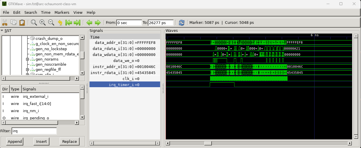
You can view the simulation traces by calling
$ gtkwave sim.fst
Performance Counters
====================
Cycles: 475
Instructions Retired: 261
The -t parameter in the simulation command line instructs Verilog to create a trace file
in FST format. Similar to a Value Change Dump file or VCD, the FST collects the activities
of every signal in the simulation. It can be viewed using GTKWave, an stand-alone
VCD/FST waveform viewer. The waveform below shows the instruction bus and the data bus.
The core is activated by a timer interrupts. Through the waveform diagram, the exact
behavior per clock cycle can be evaluated, while the firmware is executing. As we will
design hardware accelerator modules, the ability to simulate and inspect low-level
behavior at the cycle-accurate hardware level will be very useful.
$ gtkwave sim.fst
Important
The IBEX has a path to implementation, as well. In this lecture, we focus on (co)simulation of IBEX software and custom hardware modules. Hardware implementation will be covered later.
SoC Hardware Interfaces
We are now ready to discuss the SoC hardware interfaces that are relevant to this course. In this lecture, we will focus on memory-mapped hardware. That is the most generic form on SoC interfacing, and it only requires us to understand the IBEX on-chip bus.
Memory-mapped Interface
In a memory-mapped interface, hardware is integrated on the same memory bus as other on-chip memories. The idea of a memory-mapped interface is to define a hardware register that can be written using a memory-write operation on the SoC bus, and that can be read using a memory-read operation. Hence, a memory-mapped interface is a mechanism to allocate a hardware register into the memory space of a processor.
We will illustrate the memory-mapped interface in IBEX through the
operation of the Hello World example, and its access of the timer.
First, let’s see how the timer is used in the C program.
Inspect ibex/examples/sw/simple_system/hello_test/hello_text.v
and locate the main activity.
timer_enable(2000);

uint64_t last_elapsed_time = get_elapsed_time();

while (last_elapsed_time <= 4) {
  uint64_t cur_time = get_elapsed_time();
  if (cur_time != last_elapsed_time) {
    last_elapsed_time = cur_time;

    if (last_elapsed_time & 1) {
      puts("Tick!\n");
    } else {
      puts("Tock!\n");
    }
 }
 asm volatile("wfi");
}
This program waits for timer interrupts from a period timer that is set
at a timeout count of 2000 cycles. Every four timer ticks, the program
will print either the string Tick! or else the string Tock!.
The inline assembly instruction wfi (wait for interrupt) puts
the core asleep until the next timer interrupt arrives.
However, we are interested in the activities on the timer itself.
The timer interrupt service routine is located in ../common/simple_system_common.c
relative to the main program. At the end of this file, you will find the
following C code.
inline static void increment_timecmp(uint64_t time_base) {
  uint64_t current_time = timer_read();
  current_time += time_base;
  timecmp_update(current_time);
}

uint64_t timer_read(void) {
  uint32_t current_timeh;
  uint32_t current_time;
  // check if time overflowed while reading and try again
  do {
    current_timeh = DEV_READ(TIMER_BASE + TIMER_MTIMEH, 0);
    current_time = DEV_READ(TIMER_BASE + TIMER_MTIME, 0);
  } while (current_timeh != DEV_READ(TIMER_BASE + TIMER_MTIMEH, 0));
  uint64_t final_time = ((uint64_t)current_timeh << 32) | current_time;
  return final_time;
}

void timecmp_update(uint64_t new_time) {
  DEV_WRITE(TIMER_BASE + TIMER_MTIMECMP, -1);
  DEV_WRITE(TIMER_BASE + TIMER_MTIMECMPH, new_time >> 32);
  DEV_WRITE(TIMER_BASE + TIMER_MTIMECMP, new_time);
}

uint64_t get_elapsed_time(void) { return time_elapsed; }

void simple_timer_handler(void) __attribute__((interrupt));

void simple_timer_handler(void) {
  increment_timecmp(time_increment);
  time_elapsed++;
}
The timer ISR is called simple_timer_handler which itself calls a
function increment_timecmp() which reprograms the timer. The
reprogramming first reads the current timestamp (timer_read())
followed by loading it with an updated timeout value
(timecmp_update()). Each of these functions eventually boil down
to calling DEV_READ and DEV_WRITE. These are memory mapped
operations. Note that these DEV_READ and DEV_WRITE operations
are macros; they expand into memory read/write operations.
#define DEV_WRITE(addr, val) (*((volatile uint32_t *)(addr)) = val)
#define DEV_READ(addr, val) (*((volatile uint32_t *)(addr)))
So in summary, for each timer interrupt, the timer will be
reprogrammed, and the reprogramming operation consists of three memory
reads followed by three memory writes to addresses allocated to the
timer. These addresses are expressed as offsets from a
TIMER_BASE, such as TIMER_BASE + TIMER_MTIMEH and
TIMER_BASE + TIMER_MTIMECMPH. Now, we can trace these timer
operations in the FST waveform generated during the simulation. The
following shows the output of gtkwave, with some of the timer
peripheral interface signals added to the waveform diagram.
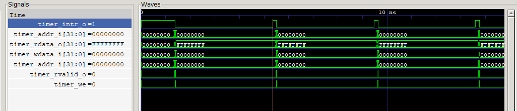
timer_intr_o: Interrupt request signal to the processortimer_addr_i: Address coming from the processor to the timer peripheraltimer_rdata_o: Data read from timer peripheral to processortimer_wdata_i: Data written to the timer peripheral from processortimer_rvalid_o: Read operation on the timer peripheraltimer_we: Write operation into the timer peripheral
We can clearly identify the periodic interrupt. Zooming on one such
periodic interrupt, you can identify the three read operations
followed by the three write operations. That is evidence, in fact,
that the processor is running the functions timer_read() and
timecmp_update().
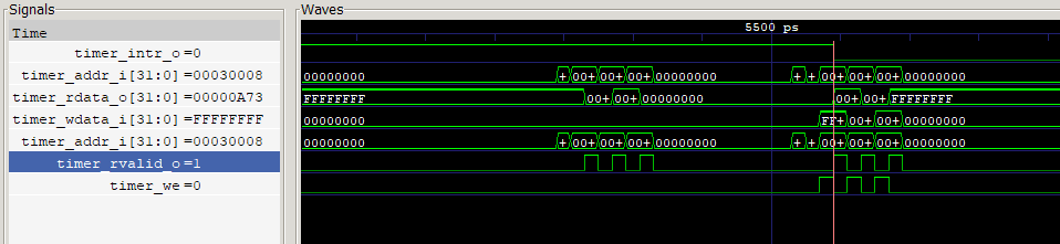
The cursor is positions at moment of the first write operation to the timer, namely:
DEV_WRITE(TIMER_BASE + TIMER_MTIMECMP, -1);
Finally, now that we are able to connect the hardware execution to the software
C code, we can also inspect the SystemVerilog of the actual timer module.
The timer module is located in shared/rtl/timer.sv. We include the full module
below to highlight the various sections of the timer.
  1// Copyright lowRISC contributors.
  2// Licensed under the Apache License, Version 2.0, see LICENSE for details.
  3// SPDX-License-Identifier: Apache-2.0
  4
  5// Example memory mapped timer
  6
  7`include "prim_assert.sv"
  8
  9module timer #(
 10  // Bus data width (must be 32)
 11  parameter int unsigned DataWidth    = 32,
 12  // Bus address width
 13  parameter int unsigned AddressWidth = 32
 14) (
 15  input  logic                    clk_i,
 16  input  logic                    rst_ni,
 17  // Bus interface
 18  input  logic                    timer_req_i,
 19
 20  input  logic [AddressWidth-1:0] timer_addr_i,
 21  input  logic                    timer_we_i,
 22  input  logic [ DataWidth/8-1:0] timer_be_i,
 23  input  logic [   DataWidth-1:0] timer_wdata_i,
 24  output logic                    timer_rvalid_o,
 25  output logic [   DataWidth-1:0] timer_rdata_o,
 26  output logic                    timer_err_o,
 27  output logic                    timer_intr_o
 28);
 29
 30  // The timers are always 64 bits
 31  localparam int unsigned TW = 64;
 32  // Upper bits of address are decoded into timer_req_i
 33  localparam int unsigned ADDR_OFFSET = 10; // 1kB
 34  // Register map
 35  localparam bit [9:0] MTIME_LOW = 0;
 36  localparam bit [9:0] MTIME_HIGH = 4;
 37  localparam bit [9:0] MTIMECMP_LOW = 8;
 38  localparam bit [9:0] MTIMECMP_HIGH = 12;
 39
 40  logic                 timer_we;
 41  logic                 mtime_we, mtimeh_we;
 42  logic                 mtimecmp_we, mtimecmph_we;
 43  logic [DataWidth-1:0] mtime_wdata, mtimeh_wdata;
 44  logic [DataWidth-1:0] mtimecmp_wdata, mtimecmph_wdata;
 45  logic [TW-1:0]        mtime_q, mtime_d, mtime_inc;
 46  logic [TW-1:0]        mtimecmp_q, mtimecmp_d;
 47  logic                 interrupt_q, interrupt_d;
 48  logic                 error_q, error_d;
 49  logic [DataWidth-1:0] rdata_q, rdata_d;
 50  logic                 rvalid_q;
 51
 52  // Global write enable for all registers
 53  assign timer_we = timer_req_i & timer_we_i;
 54
 55  // mtime increments every cycle
 56  assign mtime_inc = mtime_q + 64'd1;
 57
 58  // Generate write data based on byte strobes
 59  for (genvar b = 0; b < DataWidth / 8; b++) begin : gen_byte_wdata
 60
 61    assign mtime_wdata[(b*8)+:8]     = timer_be_i[b] ? timer_wdata_i[b*8+:8] :
 62                                                       mtime_q[(b*8)+:8];
 63    assign mtimeh_wdata[(b*8)+:8]    = timer_be_i[b] ? timer_wdata_i[b*8+:8] :
 64                                                       mtime_q[DataWidth+(b*8)+:8];
 65    assign mtimecmp_wdata[(b*8)+:8]  = timer_be_i[b] ? timer_wdata_i[b*8+:8] :
 66                                                       mtimecmp_q[(b*8)+:8];
 67    assign mtimecmph_wdata[(b*8)+:8] = timer_be_i[b] ? timer_wdata_i[b*8+:8] :
 68                                                       mtimecmp_q[   DataWidth+(b*8)+:8];
 69  end
 70
 71  // Generate write enables
 72  assign mtime_we     = timer_we & (timer_addr_i[ADDR_OFFSET-1:0] == MTIME_LOW);
 73  assign mtimeh_we    = timer_we & (timer_addr_i[ADDR_OFFSET-1:0] == MTIME_HIGH);
 74  assign mtimecmp_we  = timer_we & (timer_addr_i[ADDR_OFFSET-1:0] == MTIMECMP_LOW);
 75  assign mtimecmph_we = timer_we & (timer_addr_i[ADDR_OFFSET-1:0] == MTIMECMP_HIGH);
 76
 77  // Generate next data
 78  assign mtime_d    = {(mtimeh_we    ? mtimeh_wdata    : mtime_inc[63:32]),
 79                       (mtime_we     ? mtime_wdata     : mtime_inc[31:0])};
 80  assign mtimecmp_d = {(mtimecmph_we ? mtimecmph_wdata : mtimecmp_q[63:32]),
 81                       (mtimecmp_we  ? mtimecmp_wdata  : mtimecmp_q[31:0])};
 82
 83  // Generate registers
 84  always_ff @(posedge clk_i or negedge rst_ni) begin
 85    if (~rst_ni) begin
 86      mtime_q <= 'b0;
 87    end else begin
 88      mtime_q <= mtime_d;
 89    end
 90  end
 91
 92  always_ff @(posedge clk_i or negedge rst_ni) begin
 93    if (~rst_ni) begin
 94      mtimecmp_q <= 'b0;
 95    end else if (mtimecmp_we | mtimecmph_we) begin
 96      mtimecmp_q <= mtimecmp_d;
 97    end
 98  end
 99
100  // interrupt remains set until mtimecmp is written
101  assign interrupt_d  = ((mtime_q >= mtimecmp_q) | interrupt_q) & ~(mtimecmp_we |    mtimecmph_we);
102
103  always_ff @(posedge clk_i or negedge rst_ni) begin
104    if (~rst_ni) begin
105      interrupt_q <= 'b0;
106    end else begin
107      interrupt_q <= interrupt_d;
108    end
109  end
110
111  assign timer_intr_o = interrupt_q;
112
113  // Read data
114  always_comb begin
115    rdata_d = 'b0;
116    error_d = 1'b0;
117    unique case (timer_addr_i[ADDR_OFFSET-1:0])
118      MTIME_LOW:     rdata_d = mtime_q[31:0];
119      MTIME_HIGH:    rdata_d = mtime_q[63:32];
120      MTIMECMP_LOW:  rdata_d = mtimecmp_q[31:0];
121      MTIMECMP_HIGH: rdata_d = mtimecmp_q[63:32];
122      default: begin
123        rdata_d = 'b0;
124        // Error if no address matched
125        error_d = 1'b1;
126      end
127    endcase
128  end
129
130  // error_q and rdata_q are only valid when rvalid_q is high
131  always_ff @(posedge clk_i) begin
132    if (timer_req_i) begin
133      rdata_q <= rdata_d;
134      error_q <= error_d;
135    end
136  end
137
138  assign timer_rdata_o = rdata_q;
139
140  // Read data is always valid one cycle after a request
141  always_ff @(posedge clk_i or negedge rst_ni) begin
142    if (!rst_ni) begin
143      rvalid_q <= 1'b0;
144    end else begin
145      rvalid_q <= timer_req_i;
146    end
147  end
148
149  assign timer_rvalid_o = rvalid_q;
150  assign timer_err_o    = error_q;
151
152  // Assertions
153  `ASSERT_INIT(param_legal, DataWidth == 32)
154endmodule
Line 9-27 shows the interface of the memory mapped module. This interface is the same for every memory mapped module. It defines an address and data bus, as well as a set of control signals to define read/write operations. Note that there are both read-data and write-data bus lines: on-chip digital signals are typically unidirectional, so that we need two data busses: one for write and one for read.
Line 72-75 show the write address decoding. This is where the write-control signal for each memory mapped register is created. There are four such registers. The actual write operations on the registers are in line 83-98. These are 64-bit registers, such that there two 32-bit memory-mapped locations (LOW and HIGH) for each register.
Line 114-128 show the read address decoding. In this case, data is sent from the internal registers to the processor over
rdata_d, according to the memory address provided throughtimer_addr_i.The interrupt logic is show on Line 101. An interrupt is asserted when the timer counter exceeds the timer bound in
mtimecmp_q.Read/write operations from the memory bus to the timer have to follow the proper memory bus protocol. For this reason, there are additional delays and internal logic added, such as in line 130-147.
In our experiments, we will typically start from a working memory-mapped interface for a hardware peripheral, and customize that peripheral further to our need.