Attention
This document was last updated Nov 25 24 at 21:59
RTL Synthesis
Important
The purpose of this lecture is as follows.
To describe the role of synthesis in the digital hardware design
To provide examples of hardware inference in SystemVerilog
To experiment with an RTL synthesis tool
Attention
The example discussed in this lecture is available on https://github.com/wpi-ece574-f24/ex-expressions
Synthesis and Optimization
In the introductory lecture, we spoke about the powerful concept of modeling to abstract design activities to a higher level. There are three abstraction levels that are important to us for this lecture.
System-level: Captures a behavioral description of a hardware design. Behavior, in this context, doesn’t have to be represented as a sequential C program. Think for example on Models of Compution, which allow to express abstract, complex events such as distributed, data-driven processing (dataflow), or interacting parallel processes (process networks).
Register-transfer level: Captures a mixed behavioral/structural description of a hardware design in terms of activities of a single clock cycle, a Register Transfer. RTL is the golden model in hardware design for the past 40 years: it expresses detailed, single-bit operations while at the same time it can also capture complex decision making logic such as with if-then-else statements.
Gate-level: Captures a structural description of a hardware design in terms of low-level primitives such as a gate or a standard cell. Most of our examples have been using SKY130 standard cells. The gate-level abstraction is technology specific and therefore very well suited for performance assessments such as area, critical path delay, power.
A fourth abstraction level, the transistor-level, is of great importance to analog and mixed-signal design, but it is less commonly used in digital hardware design. We will focus on the first three.
Defining Synthesis and Optimization
The design process of a digital hardware design requires a systematic mapping and refinement from higher abstraction levels to lower abstraction levels. Synthesis and Optimization playa critical role in this process.
Attention
- Synthesis in digital hardware design involves methods that offer
a systematic (and often, automated) translation from a higher abstraction level to a lower abstraction level. The appeal of synthesis is that, once its automated, it can claim to create designs that are correct by construction.
- Optimization in digital hardware design involves methods that
transform a given abstraction level into a more optimal representation at the same abstraction level. The optimality criterium depends on the objective of the optimization. An important observation is that the abstraction level does not change.
In digital hardware design, there is Synthesis and Optimization at any abstraction level, as the following examples illustrate.
System-level synthesis will generate RTL automatically from a system-level description. For example, we can expand a dataflow diagram automatically into an RTL description. System-level optimization will transform a system-level description into a different, more optimal one. For example, we could transform a process network by instantiating multiple parallel copies of a process to increase the processing parallellism.
RTL synthesis is used to create a gate-level netlist automatically from an RTL description. For example, we can convert a Finite State Machine Description into a gate-level netlist by selecting a state encoding, and performing logic synthesis for each state transition. RTL optimization is used to create better designs. For example, we can optimize an FSM at the RTL by trying to reduce the number of states it uses. The optimization knob of RTL lies in non-technological factors, such as reducing a clock cycle on a schedule, sharing an operator, rewriting a complex expression, and so on.
Gate-level synthesis is used to convert a gate-level netlist into a layout (ie. a transistor netlist with spatial dimensions). The term gate-level synthesis is not used; instead, terms like place-and-route and clock-tree-synthesis are used. Gate-level optimization is used to improve the performance of the design, and automatic retiming would serve as a good example. The optimization know of gate-level optimization is technological, and involves transformations that reduce area, critical path, power, and so forth.
The Hardware Design Flow
We thus can define a hardware design flow that combines optimization and synthesis as shown in the next figure. This is generic as it tries to cover multiple many cases of hardware design. At each level, a design goes through multiple iterations of optimization, and finally expands towards a lower level through synthesis. These steps are largely automated at the lower layers of abstraction, while they remain largely manual at the higher layers of abstraction. One exception would be high-level synthesis, which can map a subset of system-level behaviors into RTL.
The verification flow uses simulation or symbolic (formal) techniques to check the correctness of a design. Ideally, one would use a single verification technique throughout the design but in practice, only the RTL and gate-level verification are well integrated in simulation.

The first few steps in system level synthesis and optimization are, in general, extremely hard, and they require lots of design experience. Just consider the following problem as an illustration: given a set of design constraints (such as type of computations and real-time performance) how do you choose between an FPGA, a programmable processor, a customized processor (e.g DSP), a multi-core design, or a full dedicated ASIC? In a few extreme cases, the choice may be obvious, but in general, you will find that you can always make it work with any of these components, or a combination of them. Yet, that is the choice faced by a system designer. We will revisit this problem later in the course.
Register Transfer Level Design in Verilog
We discussed RTL modeling in our previous handson assignments. In the following, we will highlight some of the key ideas and point out various pitfalls of RTL coding. A first important observation is that hardware synthesis from RTL uses two distinct mechanisms.
Hardware instantiation is used when a lower level primitive is referenced structurally in the high level design. Hardware instantiation is seen, for example, in the gate-level netlists produced during RTL synthesis. The following example instantiates a module with name
_2_of typesky130_fd_sc_hd__dfxtp_1– which is of course a flip-flop of the standard cell library. There is nothing special about instantiation, but it is often uses when complex primitives such as RAM modules must be integrated directly into the design.
sky130_fd_sc_hd__dfxtp_1 _2_ (
  .CLK(clk),
  .D(_0_),
  .Q(q)
);
Hardware inference is used when a lower level primitive will replace an RTL expression or construction. Hardware inference is a selective process, and not every Verilog construction has a corresponding hardware inference. This is an important observation, as it implies that not every Verilog construction in simulation will also lead to hardware. In fact, we will see examples where the hardware inference can lead to an implementation that differs from the simulation.
RTL coding Guidelines
RTL coding guidelines are vendor-specific; constructions that are supported by one vendor (or technology) may not be supported by another vendor. Also, the target technology may be slightly different from one vendor to the next (FPGA versus standard cells, for example). Therefore, it is crucial to rely on vendor documentation for details. Several links to such RTL Coding Guidelines are listed on top of this lecture among the Reading links.
Important
The fundamental insight of effective RTL coding is the following. It’s not helpful to think of RTL synthesis as a magical box that converts RTL code into a gate netlist. That strategy doesn’t work well on large systems. Sooner or later, you’ll end up with a buggy design (e.g., a design that mixes latches with flip-flops) and it’ll be hard to explain went wrong.
The right way of thinking about RTL inference is to think about your hardware implementation first, and then map that back to RTL code. Thus, you use RTL just as a shorthand for something that, at least in your mind, is already very structured. Hardware design is fundamentally a bottom-up process,
Visualizing the Synthesis Result
We will make use of the Cadence Genus tool for RTL synthesis. Refer to canvas for a set of slides that discuss the typical flow in cadence. Here, we will focus on the application of Genus on to implement small example.
Attention
You can download the code examples on the class design server using git.
git clone git@github.com:wpi-ece574-f24/ex-expressions.git
Once you download the code, inspect the following two files first:
syn/genus_script.tcl and constraints/constraints_comb.sdc
The synthesize the example code, run genus with the graphical user
interface option enabled (genus -gui). Then, follow along below
as we synthesize each example.
There are three levels that are relevant for visualization.
RTL. After first parsing a Verilog file, the RTL is broken down into fundamental statements and register transfers. While this is not quite a netlist yet, we can represent the RTL operations as nodes in a graph, with edges carrying dependencies between variables.
Generic Gates. After synthesis, the RTL is converted into logic gates. Most RTL synthesis tools, including
yosys, map the RTL to a generic technology, meaning a technology of gates that does not specify a specific feature size.Technology Gates. After technology mapping, the netlist of generic logic gates is converted into concrete cells from a standard cell library.
Let’s look at the following example of a basic XOR gate.
module ex1(output logic q, input logic a, input logic b);
 assign q = (a & ~b) | (~a & b);
endmodule
To synthesize this code, run the following commands in the genus prompt. These commands can be found as well in the genus_script.tcl file.
# these are initialization commands that have to be run once.
# we will run synthesis against cadence 45nm standard cells

set_db init_lib_search_path /opt/cadence/libraries/gsclib045_all_v4.7/gsclib045/timing/
read_libs slow_vdd1v0_basicCells.lib


# this sets the 'effort' of the synthesis tool: how hard it tries to find a good solution
set_db syn_generic_effort medium
set_db syn_map_effort medium
set_db syn_opt_effort medium
Now we are ready to read in the code and synthesize it.
# read in RTL of the first example
read_hdl -language sv ../rtl/ex1.sv
elaborate
After these commands, the tool has constructed an RTL schematic of the code. You can visualize the RTL schematic in the GUI using ‘show schematic’.
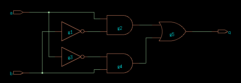
RTL netlist of ex1
# map to generic gates
set_top_module ex1
read_sdc ../constraints/constraints_comb.sdc
syn_generic
Next, we map this code to generic gates. The first two commands
set_top_module and read_sdc do housekeeping by selecting the
top module in the synthesis as well as the synthesis
constraints. syn_generic does the actual synthesis work. We will
discuss the construction of synthesis constraints in more detail while
we discuss timing. For now, it’s sufficient to understand that these
constraints are used to express the desired speed of the design. In
this case, we design the implementation to operate at 100 MHz.
# contents of constraint_comb.sdc
set non_clock_inputs [all_inputs]
set_input_delay  0 -clock clk $non_clock_inputs
set_output_delay 0 -clock clk [all_outputs]
After syn_generic completes, you’ll notice that the schematic
looks different. The generic schematic uses less cells, presumably
because these generic gates can implement a more sophisticated logic
mapping.
The following steps map the generic netlist to 130nm standard cells, and finally to an optimized netlist of 130nm standard cells.
syn_map  # map to a concrete technology
syn_opt  # optimize the implementation
After syn_opt completes, you’ll notice the resulting design
consists of a single xor cell. Because of the simplicity of this
design, the syn_opt has not practical impact: the final netlist is
the same as the mapped netlist.
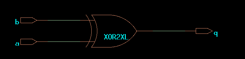
CDS45 netlist of ex1
Genus allows you to various properties of the design. The report
command, in particular, returns many useful statistics. For example,
report_area shows the active area (standard cell area) of the
final design. report_timing shows the speed (critical path) of the
final design.
@genus:design:ex1 29> report_area
============================================================
Generated by:           Genus(TM) Synthesis Solution 21.19-s055_1
Generated on:           Sep 14 2024  10:54:49 am
Module:                 ex1
Technology library:     slow_vdd1v0 1.0
Operating conditions:   PVT_0P9V_125C (balanced_tree)
Wireload mode:          enclosed
Area mode:              timing library
============================================================

Instance Module  Cell Count  Cell Area  Net Area   Total Area   Wireload
--------------------------------------------------------------------------
ex1                       1      2.736     0.000        2.736 <none> (D)
@genus:design:ex1 30> report_timing
============================================================
Generated by:           Genus(TM) Synthesis Solution 21.19-s055_1
Generated on:           Sep 14 2024  10:56:02 am
Module:                 ex1
Operating conditions:   PVT_0P9V_125C (balanced_tree)
Wireload mode:          enclosed
Area mode:              timing library
============================================================

Path 1: MET (9844 ps) Late External Delay Assertion at pin q
Group: clk
Startpoint: (F) b
Clock: (R) clk
Endpoint: (R) q
Clock: (R) clk

Capture       Launch
Clock Edge:+   10000            0
Drv Adjust:+       0            0
Src Latency:+       0            0
Net Latency:+       0 (I)        0 (I)
Arrival:=   10000            0

Output Delay:-       0
Required Time:=   10000
Launch Clock:-       0
Input Delay:-       0
Data Path:-     156
Slack:=    9844

Exceptions/Constraints:
input_delay               0              constraints_comb.sdc_line_6_1_1
output_delay              0              constraints_comb.sdc_line_7

#---------------------------------------------------------------------------------------
# Timing Point   Flags   Arc   Edge   Cell     Fanout Load Trans Delay Arrival Instance
#                                                     (fF)  (ps)  (ps)   (ps)  Location
#---------------------------------------------------------------------------------------
b              -       -     F     (arrival)      1  0.2     0     0       0    (-,-)
g18__2398/Y    -       A->Y  R     XOR2XL         1  0.0    15   156     156    (-,-)
q              -       -     R     (port)         -    -     -     0     156    (-,-)
#---------------------------------------------------------------------------------------
We will discuss the meaning of these reports in detail in later lectures. For the timing being, we will focus on three important quality metrics.
area The active area of all standard cells in the design. In this case, the active area is 2.736 square micron
cell count The number of cells in the design. In this case, the cell count is 1.
slack The margin of the design compared to the clock period. In this case, the clock period is 10000 ps, and the computation is read at 156 ps. Therefore, the slack is 9844 ps, or 9.844 ns. Slack must always be positive, otherwise your design does not meet the timing constraints; i.e. when slack is negative, your design is too slow.
In the remainder of this demonstration, we focus only on the schematics and the link from SystemVerilog to gate-level netlist.
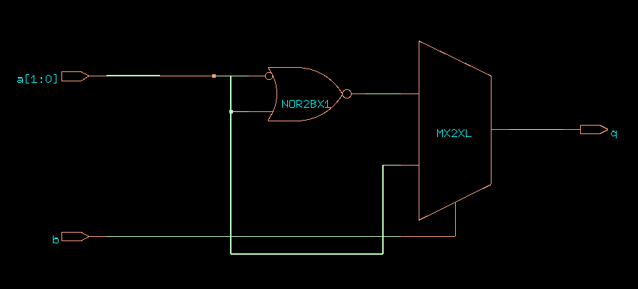
Complex Combinational Logic
A good way of creating complex combinational logic is to write expressions.
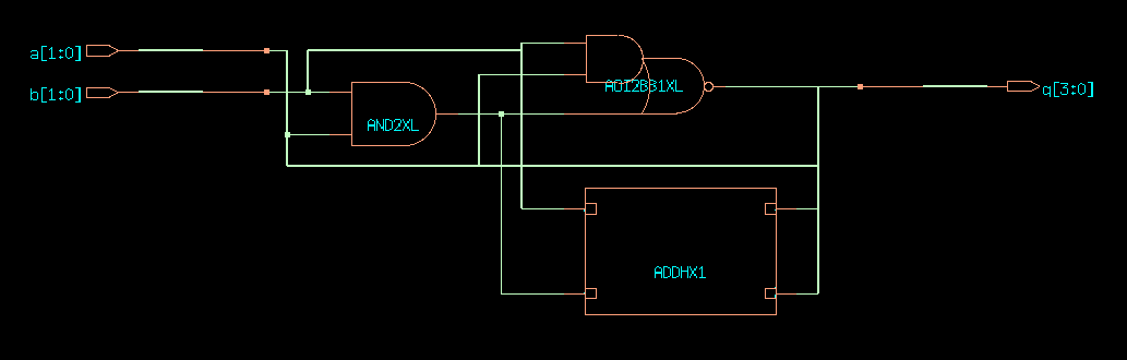
module ex2(output logic [3:0] q, input logic [1:0] a, b, c);
    assign q = a + b * c;
endmodule
This directly maps into a multiplier followed by an adder. Note how
the expression b*c has a wordlength of twice the input, as we
would expect of a multiplier. The wordlength is kept very short to
keep the resulting gate-level netlist compact enough for display.
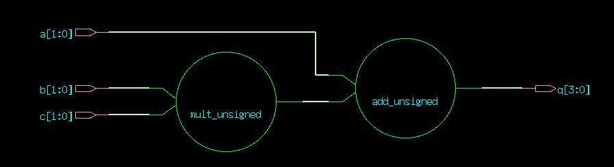
RTL netlist of ex2
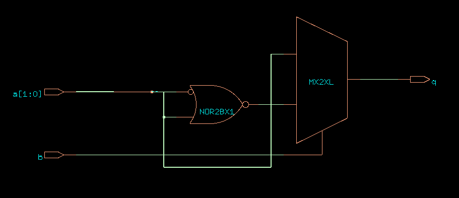
The gate-level netlist graphics uses a black bar to ungroup wires from a bus. The following is the synthesis result: a 2x2 multiplier (with 4-bit output), to which a 2-bit number is added.
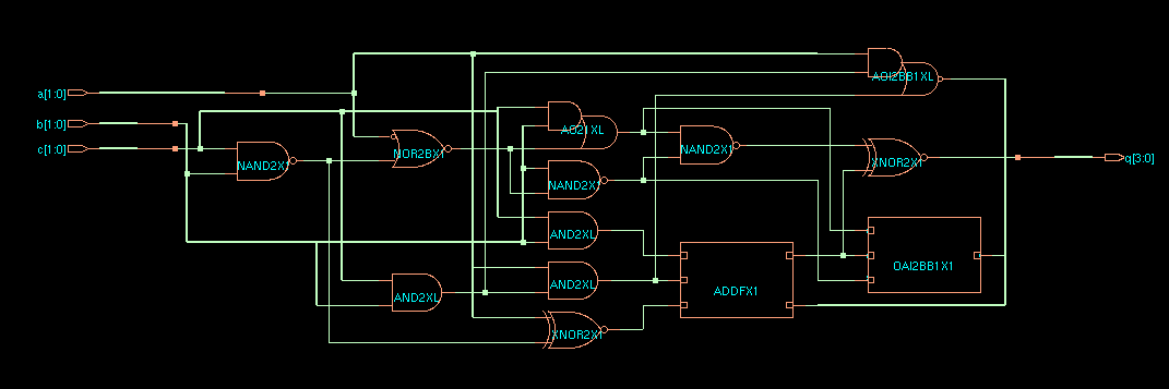
CDS45 netlist of ex2
Attention
In case you wonder about the functionality of a standard cell with
an odd or unknown name, you’d typically look into (a) the standard
cell library databook, or else the functional Verilog view of the
standard cell. For example, for OAI2BB1X1, you can find a
functional Verilog view in
/opt/cadence/libraries/gsclib045_all_v4.7/gsclib045/verilog/slow_vdd1v0_basicCells.v
on the class design server.
The RTL synthesis will use a host of tricks to make the resulting netlist as small as possible. One of these is constant propagation, where the constant inputs to a gate are used to simplify the netlist. For example, if we hardcode one input of the multiplier to the value 2, the resulting netlist can be drastically simplified. The gate level netlist implements the following design as two half-adder standard cells.
module ex3(output logic [3:0] q, input logic [1:0] a, b);
    assign q = a + b * 2;
endmodule
CDS45 netlist of ex3
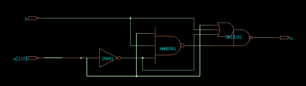
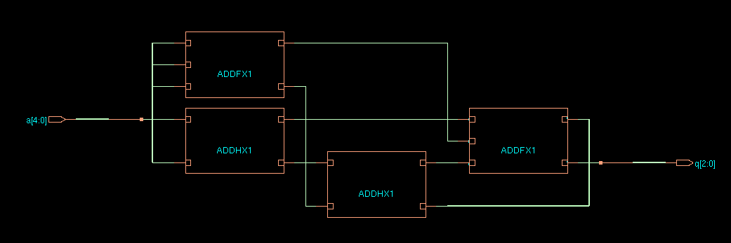
Keep in mind that some verilog operators are very expensive to
implement. For example, the inoccuous ‘modulo’ operator in Verilog
becomes a large implementation, even at a short wordlength. Again,
observe that for certain values of b (namely, at every power of 2
minus 1), the modulo operation becomes trivial to implement. The
complexity of the design stems from the fact that we want to compute
the modulo operation for any value that a two-bit number b can
take. We will have a separate lecture where we discuss the
implementation of arithmetic in detail.
module ex4(output logic [3:0] q, input logic [3:0] a, b);
    assign q = a % b;
endmodule
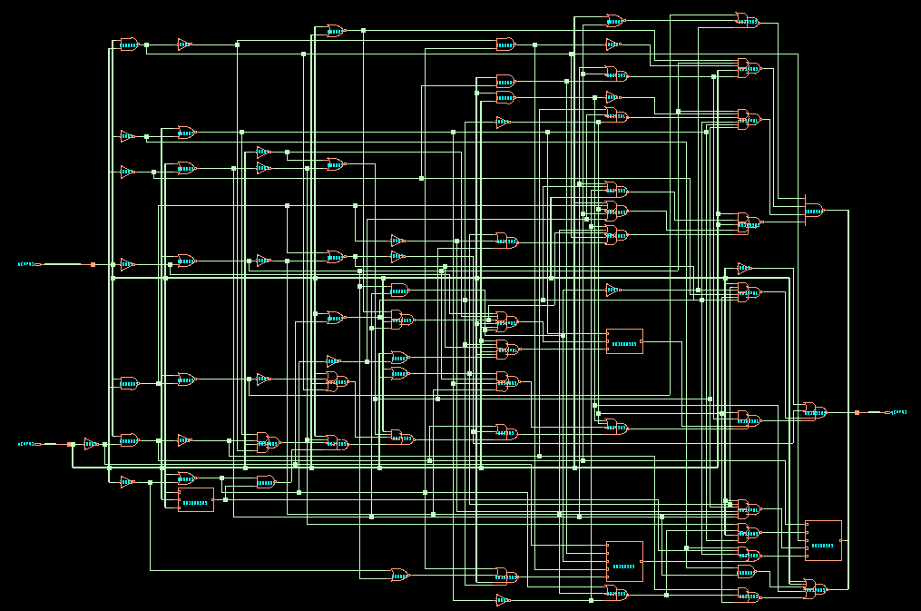
CDS45 netlist of ex4
To map combinational logic in a procedural manner, always use an
always_comb block. The initial block is not supported,
although some synthesis tools (such as for FPGA) may refer to the
initial block to determine the initial value of flip-flops. But for
combinational logic, initial remains unused. For example, the
following piece of RTL will result in a pure inverter.
module ex5(output logic q, input logic a);
    initial q = 1;
    always_comb begin
        q = ~a;
    end
endmodule
Another important point of concern with combinational logic captured
using always_comb blocks, is that the process sensitivity list
must be complete.
module ex6(output logic q, input logic a, b);
    logic t;

    always @(a) begin
        t = a ^ 1;
        q = b ^ t;
    end
endmodule
This module maps into an XNOR gate. However, looking closely at the
Verilog, this is not what was specified. If b changes, the
always block will not evaluate, thereby leaving q unmodified.
Hence, in this case, the resulting netlist is different from the
Verilog specification.
CDS45 netlist of ex6
There is an easy workaround that will make sure that this problem is
always avoided: use a wildcard for the sensitivity list of a
combinational process (always) or just use always_comb with an
empty sensitivity netlist. In other words, write the previous example
as follows. This will not have impact on the synthesis
outcome. However, it will make sure that the RTL behaves identical to
the gate-level netlist during simulation.
module ex6(output logic q, input logic a, b);
    logic t;

    always_comb begin
        t = a ^ 1;
        q = b ^ t;
    end
endmodule
Priority Logic
Priority logic is used in expressing conditions. Verilog expresses
procedural priority logic using if statements or else using
case statements. Both of these require special attention. Consider
the following design. A two-bit vector a selects either the value
of b or its complement.
module ex7(output logic q, input logic [1:0] a, input logic b);
    always_comb begin
        if (a[1])
            q = b;
        else if (a[0])
            q = ~b;
    end
endmodule
The logic generated from this code contains a latch, which is driven
by the bits of a.
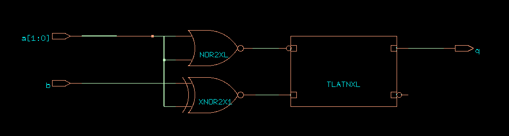
CDS45 netlist of ex7
There is a problem with the Verilog description. The netlist includes
a latch as the cell sky130_fd_sc_hd__dlxtn_1 (we intend to
describe combinational logic, not stateful logic!). That problem is
solved through a default assignment, a value that will be assigned
to q when a combination of the input values does not evaluate to a
concrete update for q. In this case, when a is 00, the
value of q is left unspecified.
module ex8(output logic q, input logic [1:0] a, input logic b);
    always_comb begin
        q = 0;
        if (a[1])
            q = b;
        else if (a[0])
            q = ~b;
    end
endmodule
This generates the following logic. The latch has disappeared.
CDS45 netlist of ex8
Note also the impact of the priority logic. In a nested if-then
case, the outer if receives priority. In the example above, bit
a[1] has priority over a[0], meaning that if the value a
is 1, then the function of this module is to copy b.
We can swap the nesting of the if-then-else statement, if we need a
different priority. In the following example, bit a[0] has
priority over a[1]. When a is 11, the function of this
module is to copy the complement of b.
module ex9(output logic q, input logic [1:0] a, input logic b);
    always_comb begin
        q = 0;
        if (a[0])
            q = ~b;
        else if (a[1])
            q = b;
    end
endmodule
CDS45 netlist of ex9
Unlike if statements, expressing priorities with case
statements is harder, because a case statement tests only a single
condition for all the branches. However, a case statement is
better at handling complex logic, such as for example with the
next-state logic of finite state machines. A case statement has
the same issue as if statements and can infer latches if an
uncovered case condition is left. The use of a default branch
ensures that the case logic is always complete.
module ex10(output logic q, input logic [1:0] a, input logic b);
    always_comb begin
        case (a)
            1: q = ~b;
            2: q = b;
            default: q = 0;
        endcase
    end
endmodule
CDS45 netlist of ex10
Loops
Verilog supports the use of loops in procedural blocks. These loops have no meaning for synthesis and will be expanded as the Verilog is translated to gates. If you want to implement a control contruction, you will have to build it using a finite state machine. The following example show how to compute the Hamming weight of a 5-bit number.
module ex11(output logic [2:0] q, input logic [4:0] a);
    logic [2:0] tmp;
    integer i;

    always_comb begin
        tmp = 0;
        for (i = 0; i < 5; i = i + 1)
            tmp = tmp + a[i];
        q = tmp;
    end
endmodule
This module results in pure combinational code. The compiler will
unroll the loop before RTL synthesis. Note also that we can assign
and reassign the value of tmp. However, for synthesis, all the
iterations in a loop will instantly execute. tmp does not play the
role of a hardware storage element.
CDS45 netlist of ex11
For example, the following modules, ex12 and ex13, will
generate gates as ex11.
module ex12(output logic [2:0] q, input logic [4:0] a);
    logic [2:0] tmp;
    integer i;

    always_comb begin
        tmp = 0;
        tmp = tmp + a[0];
        tmp = tmp + a[1];
        tmp = tmp + a[2];
        tmp = tmp + a[3];
        tmp = tmp + a[4];
        q = tmp;
    end
endmodule
module ex13(output logic [2:0] q, input logic [4:0] a);
    always_comb begin
        q = 0 + a[0] + a[1] + a[2] + a[3] + a[4];
    end
endmodule
Flip-flops
Hardware registers are modeled in a separate always block which is
driven by the clock signal. The assignment on flip-flops always
proceeds using a non-blocking assignment. A non-blocking assignment
is necessary to allow simultaneous assignments on all flip-flops. The
following example shows two flop-flops that are connected
back-to-back. The use an asynchronous reset.
module ex14(
    input wire d,
    input wire reset,
    input wire clk,
    output wire q1,
    output wire q2
);
    logic q1r, q2r;

    always_ff @(posedge clk or posedge reset) begin
        if (reset) begin
            q1r <= 1'b0;
            q2r <= 1'b0;
        end else begin
            q1r <= q2r;
            q2r <= q1r ^ d;
        end
    end

    assign q1 = q1r;
    assign q2 = q2r;
endmodule
CDS45 netlist of ex14
A flip-flop with synchronous reset is achieved by a simple change to the process sensitivity list.
module ex15(
    input logic d,
    input logic reset,
    input logic clk,
    output logic q1,
    output logic q2
);
    logic q1r, q2r;

    always_ff @(posedge clk) begin
        if (reset) begin
            q1r <= 1'b0;
            q2r <= 1'b0;
        end else begin
            q1r <= q2r;
            q2r <= q1r ^ d;
        end
    end

    assign q1 = q1r;
    assign q2 = q2r;
endmodule
CDS45 netlist of ex15
While asynchronous reset inputs are a common feature on flip-flop cells in standard cell libraries, synchronous reset are usually realized by multiplexing additional logic at the flip-flop inputs.
Gated clocks on flip-flops are to be done with caution. It’s not a good idea to directly manipulated the clock as follows. This will result in difficult skew problems.
module ex16(
    output logic q,
    input logic enable,
    input logic clk,
    input logic d
);
    logic qr;
    wire gatedclk;

    // An example of how NOT to gate a clock!
    assign gatedclk = clk & enable;

    always_ff @(posedge gatedclk) begin
        qr <= d;
    end

    assign q = qr;
endmodule
CDS45 netlist of ex16
A better way to implement a gate clock is to add an enable single inside of the synchronous update as follows. This design will ensure that each flip-flop receives a primitive clock signal.
module ex17(
    output logic q,
    input logic enable,
    input logic clk,
    input logic d
);
    logic qr;

    always_ff @(posedge clk) begin
        if (enable)
            qr <= d;
    end

    assign q = qr;
endmodule
CDS45 netlist of ex17
Finite State Machines
We already briefly discussed the design of finite state machines. We will discuss the implementation aspects by means of an example.
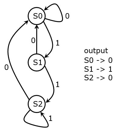
Let’s create an FSM that reencodes a bitstring as follows. The first 1 in a string of 1s is passed as a 1. Otherwise, the output is 0. The following shows an example input string with its corresponding output string.
input string:      1 1 1 0 0 1 0 0 1 1 1 0 1 1
output string:     1 0 0 0 0 1 0 0 1 0 0 0 1 0
The first step in such a design is to design a state transition diagram. The following is the design of a Moore FSM that implements this FSM.
We will discuss three different Verilog implementations for this design: a three-process style (recommended), a two-process style and a single-process style. The last two provide a more compact style, but may be a little harder to develop.
Important
Keep the following in mind when writing Verilog for FSM.
Always draw your state transition diagram before coding. The Verilog representation of a state transition diagram is messy and error prone.
Always use symbolic state encoding. The synthesis tools will choose a state encoding for you which will result in the fastest/most compact design.
Always model state transition logic as a case statement. Don’t forget a default assignment.
Always make sure that your state transition logic is complete. Add a default state transition that will bring back the finite state machine to its initial (or another known) state.
Here is a three-process model of the finite state machine. The
symbolic states are s0, s1, s2. We have assigned them a
specific value for RTL simulation purposes. However, the RTL synthesis
tool will choose a state encoding that results in the smallest
possible area. Both the next-state block and the output block have
default assignments (for the next state and for the output,
respectively).
module ex19(
    output logic q,
    input logic i,
    input logic clk,
    input logic reset
);
    logic rq;

    logic [1:0] state, state_next;

    localparam s0 = 2'b00, s1 = 2'b01, s2 = 2'b10;

    always_ff @(posedge clk or posedge reset) begin
        if (reset)
            state <= s0;
        else
            state <= state_next;
    end

    always_comb begin
        state_next = s0;
        case (state)
            s0:
                if (i == 1'b1)
                    state_next = s1;
                else
                    state_next = s0;
            s1:
                if (i == 1'b1)
                    state_next = s2;
                else
                    state_next = s0;
            s2:
                if (i == 1'b1)
                    state_next = s2;
                else
                    state_next = s0;
        endcase
    end

    always_comb begin
        rq = 1'b0;
        case (state)
            s0:  rq = 1'b0;
            s1:  rq = 1'b1;
            s2:  rq = 1'b0;
        endcase
    end

    assign q = rq;
endmodule
This implementation yields a design as shown.
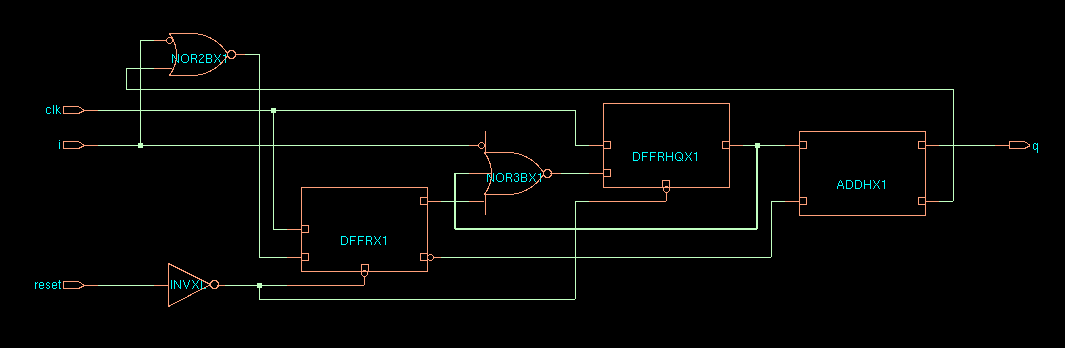
To verify that this is a correct implementation of the spec, we recompute the state transition diagram from the schematic. Note that DFF0 is the rightmost flip-flop.
DFF1 |
DFF0 |
i |
q |
Next DFF1 |
Next DFF0 |
|---|---|---|---|---|---|
0 |
0 |
0 |
0 |
0 |
0 |
0 |
0 |
1 |
0 |
0 |
1 |
0 |
1 |
0 |
1 |
0 |
0 |
0 |
1 |
1 |
1 |
1 |
0 |
0 |
0 |
0 |
0 |
0 |
0 |
0 |
0 |
1 |
0 |
1 |
0 |
1 |
1 |
0 |
0 |
0 |
0 |
1 |
1 |
1 |
0 |
0 |
0 |
From the transition table, we recreate the state transition diagram which closely matches the original specification.
Note, however, that the state 11, which did not appear in the
logical state machine, now does occur in the physical
implementation. Indeed, there is nothing that prevents both flip-flops
from storing 1 at the same time. This would occur, of course, as the
result of a fault. The important element is that this illegal state is
effectively avoided, because it will transition into state 00.
Finally, we illustrate two more compact notations for this FSM, which
are created by collapsing several processes into a single process. All
of the following Verilog descriptions map into the same identical
netlist. The first transformation is to merge the output encoding with
the next-state logic, which is implemented by merging two always
blocks into a single one.
module ex20(
    output logic q,
    input logic i,
    input logic clk,
    input logic reset
);
    logic rq;

    logic [1:0] state, state_next;

    localparam s0 = 2'b00, s1 = 2'b01, s2 = 2'b10;

    always_ff @(posedge clk or posedge reset) begin
        if (reset)
            state <= s0;
        else
            state <= state_next;
    end

    always_comb begin
        state_next = s0;
        rq = 1'b0;
        case (state)
            s0: begin
                rq = 1'b0;
                if (i == 1'b1)
                    state_next = s1;
                else
                    state_next = s0;
            end
            s1: begin
                rq = 1'b1;
                if (i == 1'b1)
                    state_next = s2;
                else
                    state_next = s0;
            end
            s2: begin
                rq = 1'b0;
                if (i == 1'b1)
                    state_next = s2;
                else
                    state_next = s0;
            end
        endcase
    end

    assign q = rq;
endmodule
The second transformation is to make it even more compact, by collapsing the
synchronous always process that takes care of register update, with the
combinational always process. This merging is tricky, since a synchronous
always process can only contain assignments to registers. Thus, we are
forced to push the output encoding out of the always process into a
dataflow statement.
module ex21(
    output logic q,
    input logic i,
    input logic clk,
    input logic reset
);
    logic [1:0] state, state_next;

    localparam s0 = 2'b00, s1 = 2'b01, s2 = 2'b10;

    always_ff @(posedge clk or posedge reset) begin
        if (reset)
            state <= s0;
        else begin
            state <= s0;
            case (state)
                s0: begin
                    if (i == 1'b1)
                        state <= s1;
                    else
                        state <= s0;
                end
                s1: begin
                    if (i == 1'b1)
                        state <= s2;
                    else
                        state <= s0;
                end
                s2: begin
                    if (i == 1'b1)
                        state <= s2;
                    else
                        state <= s0;
                end
            endcase
        end
    end

    assign q = (state == s1);
endmodule