Attention
This document was last updated Nov 25 24 at 21:59
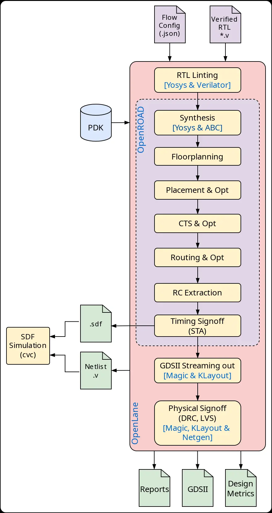
Design Flow
Important
The purpose of this lecture is as follows.
To enumerate the major steps in a digital design flow to go from RTL code to a layout
To describe a sample implementation of this flow by the example of OpenLane
To define the practical realization of a digital design flow for 574
To illustrate the role of gate-level simulation in this design flow
To provide implementation guidance such as Makefile coding and coding guidelines
To describe the FuseSoC tool for design flow construction
To illustrate a combination of FuseSoC and the standard 574 flow.
Attention
The following references are relevant background to this lecture.
Andrew Kahng et al., “VLSI Physical Design: From Graph Partitioning to Timing Closure,” Chapter 1 (Introduction), Springer Publishers
M Shalan, T. Edwards, “Building OpenLANE: A 130nm OpenROAD-based Tapeout-Proven Flow,” Proc. ICCAD 2020
Attention
Examples for this lecture are available under https://github.com/wpi-ece574-f24/ex-flow
Generic IC Design Flow
In this lecture, we take a step back and look at the big picture in Digital IC Design. The modern IC design flow is a marvel of efficiency and pragmatism. The number of hard optimization problems that are addressed by automatic tools in IC design is truly remarkable. The majority of design automation problems, such as placing of standard cells, routing a clock tree, deciding on the proper power distribution network, etc, can only be heuristically solved. Yet, without the design flow, there would be no complex chips, and no need for Moore’s law.
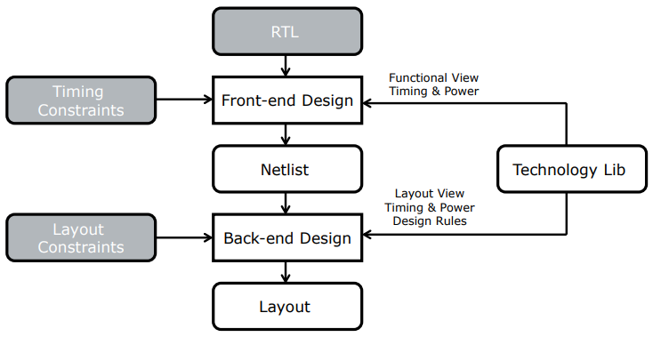
For standard cell based design (our focus on this class), different IC design flows share many common ideas and steps. We will therefore start with a discussion of a generic design flow, and afterwards refine that example into a concrete implementation based on OpenLANE, an open-source IC design flow. We start with the generic flow. There are two major phases in a design flow, generally called front-end design flow and back-end design flow. The front-end converts an HDL implementation into a netlist, i.e. a network of technology-specific logic gates, The back-end converts the netlist into a structure of place standard cells, interconnected by wires. Complexity wise, the backend is more intricate and involved than the front-end. This looks somewhat surprising, given that the main user input, the RTL, is provided at the front-end. The reality, of course, is that the design space of the back-end has many more dimensions and trade-offs than the design space of the front-end. Besides the RTL, you’ll find that design flows require a large number of constraints, technology libraries and design scripts (not shown in the figure), to guide the process of converting RTL into a netlist and afterwards into a layout.
The technology library is a crucial component to support the design flow. At high level, the technology library is a description of the standard cells and low-level technology components required to complete the chip layout. A technology library provides several different views which describe different aspects of each standard cell in that library.
A timing view and a power view allow tools to evaluate the speed and power consumption of cells after their integration in a netlist.
A functional view allows tools to simulate the functionality of the cells after their integration in a netlist.
A layout view allows tools to know the physical outline of the cell, including the location where connections should be made.
As an example, let’s take one cell from the skywater 130nm library, a
two-input NAND gate with drive strength 1. The technology library for
the skywater 130nm is located at
/opt/skywater/libraries/sky130_fd_sc_hd on the design server. The
timing and power characteristics of the two-input NAND gate is
captured in a lib file, for example
timing/sky130_fd_sc_hd__tt_025C_1v80.lib. The functional behavior
of the two-input NAND gate is captured in a Verilog file such as
cells/nand2/sky130_fd_sc_hd__nand2_1.v. The layout view of the
two-input NAND gate is captured in a LEF file such as
cells/nand2/sky130_fd_sc_hd__nand2_1.lef. We will discuss some of
these formats in further detail in future lectures. The main point,
however, is to see that a ‘standard cell’ is not an atomic
entity. Depending on what you want to achieve in the design flow
(simulation, timing evaluation, layout construction, …), different
file formats come into play that each highlight specific aspects of
the standard cell. In that sense, a ‘standard cell library’ is very
different from a traditional software library.
Design Steps in the front-end
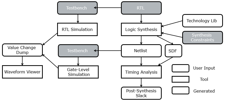
The first task in front-end design is to verify that the design is correct. This requires the design of a testbench and a simulation tool. Typically, a testbench will contain one or more tests to validate that the output of the design under test matches the expected output. For in-depth debugging purposes, a Value Change Dump (VCD) file can be produced that records every signal change over the course of the simulation. However, generating VCDs is time- and disk-space-hungry, so it is rarely done in an exhaustive manner.
A correct RTL is next mapped to a technology netlist by a logic synthesis tool. The logic synthesis tool requires a technology library containing a list of target cells, a set of synthesis constraints, and (not shown in the figure) a synthesis script. Typical synthesis constraints specify to desired clock period of the design, or the constraint to apply specific synthesis techniques (e.g. encoding finite state machine states with one-hot codes). Synthesis constraints play an important rule in the quality of the logic synthesis output.
The netlist (or gate-level netlist) can be simulated with the same testbench as the RTL design, and of course one would expect an equivalent output compared to the RTL simulation. There may be subtle differences, however. For example, the reset behavior of a gate-level netlist may not be identical to the RTL design. Also, a gate-level simulation is able to express proper technology delays (propagation delay through the gates, for example), and timing-depedent effects such as glitches may become visible at the gate-level. At the RTL, every computation step is defined by a clock cycle. At the gate-level, a computation step can be as small as a single gate transition.
Another result form the logic synthesis is a constraints file that captures the delays of the netlist (SDF). These delays are based on the actual cells used in the circuit, in combination with the fanout and specific wireload model adopted using synthesis. This SDF file will enable accurate timing simulation of the gate-level circuit. The SDF can also be used by static timing analysis (STA) tools.
Because the timing properties of a netlist are different from the (essentially untimed) RTL, the netlist can also be verified using timing analysis – which we will discuss in detail during a future lecture. The most important outcome of the timing analysis is the slack, which is the margin between the designs’ project clock period (clock frequency) and the actual delay experienced by the clock. A positive slack means that the logic is faster enough to finish a single-cycle computation within a clock period. A negative slack, however, means that the design experiences a timing violation and requires performance updates. Such updates can imply adjusting the synthesis constraints, the synthesis script, or even improving the RTL.
Design Steps in the back-end
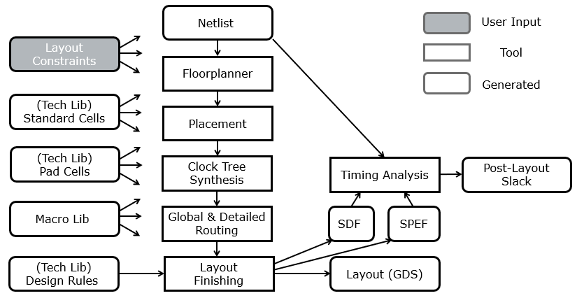
The backend starts with a design netlist that meets the clock period constraint, along with other synthesis constraints. A sequence of tools will now convert the netlist into a structure. Each tool handles a specific aspect in the definition of that structure.
A floorplanner defines the major outline characteristics of the chip, such as the regions where standard cells can be placed, where hard macro’s (memory cells) can be placed, and how input/output cells are implemented. Furthermore, the floorplanner defines the power grid infrastructure on the chip. For a chip with hundreds of thousands of cells, the power grid becomes a hierarchical network which must ensure that power is evenly distributed across the chip, such that each individual cell can operate at nominal capacity.
Next a placement tool will decide where to place the standard cells, making sure that cells with lots of local interconnections are placed together, and making sure that there is enough room between the cells to implement the interconnections.
Next, the clock signal network is created by clock tree synthesis. The clock is the single most important global net of the chip (or block). The key challenge is to make sure that the clock signal arrives at each cell (flip-flop) at the same time, and it requires the definition of a hierarchical network called a clock tree.
Next, the signal interconnections between individual gate and macro pins are implemented in the routing step. Routing is done in two phases: Global routing decides roughly on the path taken by each wire, by allocating each wire to a track of grid cells. Next, detailed routing decides on the detailed implementation of individual wires, such as the metal layers and via interconnections used.
The final step layout finishing makes sure that the layout meets all the design rules in place for the technology. Design rules specify the density and spacing of low-level chip elements such as metal wires, and polysilicon regions. The final output of the layout finishing phase is a GDS (graphic design system), a structural specification of a chip design. Another file that is produced as outcome is a new delay estimation file (SDF) in addition to a layout parasitics file (SPEF). The SDF has the same meaning as the earlier SDF produced after synthesis, except that the wireload model is now replaced by the actual interconnect delay estimates. The SDF file is used for timing analysis and post-layout gate-level simulation. The SPEF file reflects capacitance and resistance values of the layout interconnections. SPEF files are used for checks of signal integrity of the layout, as well as low-level transistor simulation.
Clearly, there are a tremendous number of parameters that play a role in moving a netlist into a layout. Multiple technology libraries support the implementation of standard cells, I/O pad cells and macro’s. Layout constraints craft the structure into a given desired shape, which must meet the design rules for the selected technology.
OpenLane: An Open Source Design Flow
Attention
This course does not express a preference on which approach is better: open-source or (commercial) closed-source. Both approaches have advantages and disadvantages, and there are good reasons for either approach.
Perhaps remarkably, all of the above tools nowadays are available as open-source components, up to and including the technology libraries. This is a very recent evolution that is having a profound impact on the hardware design process, certainly in educational context. We will discuss one example, the OpenLane Flow, which is the same design flow used for the TinyTapeout projects.
OpenLane is an extension of another open-source project called OpenROAD. The latter was initiated as a DARPA project with the objective of creating a tool chain that is able to complete an RTL-to-layout flow within 24 hours. A full day may sound a lot, if you are used to compiling C or FPGA code. But, given the complexity of this task, plus the fact that this task is entirely supported using open-source technology, this is a truly remarkable achievement which was near impossible just a few years ago. Furthermore, most smaller designs (such as the tiles in TinyTapeout projects), take far less time to implement. The following table shows that for each major design step in a chip design flow, there is now an open-source alternative.
Step |
Cadence |
OpenLane |
|---|---|---|
Logic Synthesis |
Genus |
Yosys, ABC |
ATPG |
Genus |
Fault |
Placement |
Innovus |
RePlAce, OpenDP |
Routing |
Innovus |
FastRoute, TritonRoute |
CTS |
Innovus |
TritonCTS |
Timing Analysis |
Tempus |
OpenSTA |
LVS, DRC |
Calibre (Siemens) |
Netgen, Magic |
The standard Openlane flow follows overall a flow that is similar to the generic flow presented earlier.
Attention
The following instructions walk you through an example using OpenLane. You need a good Ubuntu box or WSL2 on your laptop to be able to run this.
Installing OpenLane2
The following instructions describe an installation of OpenLane2 on docker. If you don’t have a docker installation on your laptop, follow the instructions the OpenLane2 documentation
# Remove old installations
sudo apt-get remove docker docker-engine docker.io containerd runc

# Installation of requirements
sudo apt-get update
sudo apt-get install \
   ca-certificates \
   curl \
   gnupg \
   lsb-release
# Add the keyrings of docker
sudo mkdir -p /etc/apt/keyrings
curl -fsSL https://download.docker.com/linux/ubuntu/gpg | sudo gpg --dearmor -o /etc/apt/keyrings/docker.gpg
# Add the package repository
echo \
"deb [arch=$(dpkg --print-architecture) signed-by=/etc/apt/keyrings/docker.gpg] https://download.docker.com/linux/ubuntu \
$(lsb_release -cs) stable" | sudo tee /etc/apt/sources.list.d/docker.list > /dev/null
# Update the package repository
sudo apt-get update

# Install Docker
sudo apt-get install docker-ce docker-ce-cli containerd.io docker-compose-plugin

# Check for installation
sudo docker run hello-world
If all goes well, you will see a ‘Hello from Docker!’ message printed by the last command.
Many of the Openlane commands require the user to be a member of the docker group (with sudo privileges!). The following commands make this happen.
sudo groupadd docker
sudo usermod -aG docker $USER
sudo reboot # REBOOT!
Once you have docker running, you can now download and install the openlane container:
python3 -m pip install openlane
Followed by a simple test:
python3 -m openlane --dockerized --smoke-test
Running OpenLane2
Attention
This example code is also available on the repository https://github.com/wpi-ece574-f24/ex-flow.git
The following is a multiply-accumulate module that we will implement
using the openlane2 flow. The design accepts two variables x1 and
x2 and computes the product as well as the accumulated
product. The output of the design is 10 bit, and the product is
internally rescaled so that only the 10 most significant bits are
kept.
 module mac(
  input [7:0] x1,
  input [7:0] x2,
  output reg [9:0] y,
  output reg [9:0] m,
  input  reset,
  input  clk
);

 reg [9:0] y_next;
 reg [15:0] m16;

 always @(posedge clk)
     if (reset)
       y <= 10'b0;
     else
       y <= y_next;

 always @(*)
   begin
      m16 = x1 * x2;
      m = m16[15:6];
      y_next = y + m;
   end

endmodule
To build a chip for this Verilog file, we must provide a configuration file to tell Openlane about the physical characteristics of the chip. The overall flow is set up such that it will run the entire frontend and backend in one iteration. Furthermore, this implementation does not include simulation/validation of the design, which would have to be completed separately.
The following is an example configuration file for the multiply-accumulate chip.
{
 "DESIGN_NAME": "mac",
 "VERILOG_FILES": "dir::src/mac.v",
 "CLOCK_PORT": "clk",
 "CLOCK_PERIOD": 100,
 "pdk::sky130A": {
   "MAX_FANOUT_CONSTRAINT": 6,
   "FP_CORE_UTIL": 40,
   "PL_TARGET_DENSITY_PCT": "expr::($FP_CORE_UTIL + 10.0)",
   "scl::sky130_fd_sc_hd": {
     "CLOCK_PERIOD": 15
    }
  }
}
In a nutshell, this configuration file indicates the source code files that make up the design, and the selection of the target technology along with physical constraints for the design. The two most important variables are the clock period, and floorplan target utilization (the ratio of the standard cell active area to the total core). There are a great number of additional configurarion variables available that help you handle many other aspects of the design. They are described in detail in online documentation
To implement the design, first start the openlane docker container:
python3 -m openlane --dockerized
And next, run the design flow.
openlane config.json
The flow runs through a great number of individual steps, but every
step along the way is documented in a log. These logs can be consulted
in the runs subdirectory after the flow completes.
OpenLane Container (2.1.8):/home/pschaumont/ex-flow/openlane2/runs/RUN_2024-09-26_14-45-48% ls
01-verilator-lint                   27-openroad-globalplacement       53-openroad-irdropreport
02-checker-linttimingconstructs     28-odb-writeverilogheader         54-magic-streamout
03-checker-linterrors               29-checker-powergridviolations    55-klayout-streamout
04-checker-lintwarnings             30-openroad-stamidpnr             56-magic-writelef
05-yosys-jsonheader                 31-openroad-repairdesignpostgpl   57-odb-checkdesignantennaproperties
06-yosys-synthesis                  32-openroad-detailedplacement     58-klayout-xor
07-checker-yosysunmappedcells       33-openroad-cts                   59-checker-xor
08-checker-yosyssynthchecks         34-openroad-stamidpnr-1           60-magic-drc
09-checker-netlistassignstatements  35-openroad-resizertimingpostcts  61-klayout-drc
10-openroad-checksdcfiles           36-openroad-stamidpnr-2           62-checker-magicdrc
11-openroad-checkmacroinstances     37-openroad-globalrouting         63-checker-klayoutdrc
12-openroad-staprepnr               38-openroad-checkantennas         64-magic-spiceextraction
13-openroad-floorplan               39-odb-diodesonports              65-checker-illegaloverlap
14-odb-checkmacroantennaproperties  40-openroad-repairantennas        66-netgen-lvs
15-odb-setpowerconnections          41-openroad-stamidpnr-3           67-checker-lvs
16-odb-manualmacroplacement         42-openroad-detailedrouting       68-checker-setupviolations
17-openroad-cutrows                 43-odb-removeroutingobstructions  69-checker-holdviolations
18-openroad-tapendcapinsertion      44-openroad-checkantennas-1       70-checker-maxslewviolations
19-odb-addpdnobstructions           45-checker-trdrc                  71-checker-maxcapviolations
20-openroad-generatepdn             46-odb-reportdisconnectedpins     72-misc-reportmanufacturability
21-odb-removepdnobstructions        47-checker-disconnectedpins       error.log
22-odb-addroutingobstructions       48-odb-reportwirelength           final
23-openroad-globalplacementskipio   49-checker-wirelength             flow.log
24-openroad-ioplacement             50-openroad-fillinsertion         resolved.json
25-odb-customioplacement            51-openroad-rcx                   tmp
26-odb-applydeftemplate             52-openroad-stapostpnr            warning.log
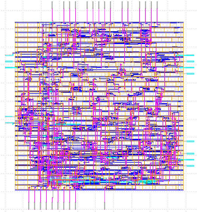
In the final subdirectory, the layout file is available as
final/gds/mac.gds. You can open this file in the klayout
viewer which is part of openlane. Once inside KLayout, you can also
load a layer properties file which replaces the abstract numbered
layers with names. For SKY130, there’s such a layer properties file
included in the example code. The following shows the layout in
klayout, when all metal layers (drawing) are enables, as well as local
interconnect, polysilicon, and the cell outline. It’s easy to spot
large empty areas in the middle with cells that are no connected to
any net. Such cells as filler cells, they are there to ensure to
that the power rails on metal1 are connected across the entire row of
standard cells.
klayout final/gds/mac.gds
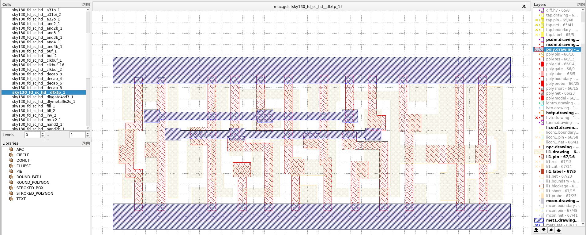
Because the view offered by klayout is purely structural, it is not easy to connect the layout to the higher level properties of the design (such as net names, or names of registers). On the other hand, klayout allows you to inspect the layout of individual standard cells. You can do this by selecting one of the standard cells in the design hierarchy and set that as the new design top in klayout. For example, the following shows a flip-flop layout.
Standard 574 Design Flow
In this course, we are building a flow from Cadence tools. Also, we are studying individual aspects of the design flow separately, and this reflects how we organize the data files.
In the following example, we demonstrate the directory structure for the frontend.
.
├── constraints
│   └── constraints_clk.sdc
├── glsim
│   ├── Makefile
│   └── tb.sv
├── rtl
│   └── mac.sv
├── sim
│   ├── Makefile
│   └── tb.sv
├── sta
│   ├── Makefile
│   └── tempus.tcl
└── syn
    ├── genus_script.tcl
    └── Makefile
The source code of the design is stored in rtl. The code can be
simulated with the testbench tb.sv under sim.
RTL Simulation
The following is the testbench tb.sv. Note the following aspects.
The testbench records a value change dump (VCD) that allow inspection
of the simulation using a waveform viewer such as gtkwave. The
testbench applies pseudorandom stimuli, but also verifies the
correctness of the results generated.
module tb;
logic [7:0] x1;
logic [7:0] x2;
logic [9:0] m;
logic [9:0] y;
logic reset;
logic clk;

mac dut(.x1(x1),
        .x2(x2),
        .m(m),
        .y(y),
        .reset(reset),
        .clk(clk));

always
begin
   clk = 1'b0;
   #5 clk = 1'b1;
   #5;
end

logic [15:0] test_m;
logic [9:0] test_y;

initial
begin
   $dumpfile("trace.vcd");
   $dumpvars(0, tb);
   x1 = 8'b0;
   x2 = 8'b0;
   test_m = 10'b0;
   test_y = 10'b0;

   reset = 1'b1;
   repeat(3)
      @(posedge clk);
   #1;
   reset = 1'b0;

   $display("m %d y %d", m, y);

   repeat(30)
     begin
        x1 = $random;
        x2 = $random;
        @(posedge clk);
        #1;

        test_m = (x1 * x2) >> 6;
        test_y = test_y + test_m;
        $display("x1 %d x2 %d m %d y %d exp_m %d exp_y %d ERR %d",
                 x1, x2, m, y, test_m, test_y, ~((test_m == m) && (test_y == y)));
        #1;
     end // repeat (30)

   $finish;
end

endmodule
To understand the simulation command, inspect the Makefile. The
general principle of the ECE574 flow is to drive all implementation
steps from a Makefile which will call the simulator with the proper
command line parameters.
This particular makefile has two targets: sim and simg. For
batchmode simulation, use make sim. To access the simulator GUI,
use make simg.
RTL Synthesis
Building a gate-level netlist for the multiply-accumulate requires synthesis constraints as well as a synthesis script.
The synthesis constraints are stored under
constraints/constraints_clk.sdc. Constraints include the clock
period, as well as the input delay and output delay for ports. The
constraints file is written in such a way that the user can provide a
clock period value through an environment variable CLOCKPERIOD.
if {![info exists ::env(CLOCKPERIOD)] } {
   set clockPeriod 20
} else {
   set clockPeriod [getenv CLOCKPERIOD]
}

create_clock -name clk -period $clockPeriod [get_ports "clk"]

set_input_delay  0 -clock clk [all_inputs -no_clocks]
set_output_delay 0 -clock clk [all_outputs]
The use of environment variables allows you to develop scripts that can serve multiple designs and multiple purposes. In a Makefile we frequently rely on environment variables as well, to define tool parameters and options.
Consider the Makefile in the syn subdirectory.
all: syn

syn:
     BASENAME=mac \
     CLOCKPERIOD=4 \
     TIMINGPATH=/opt/cadence/libraries/gsclib045_all_v4.7/gsclib045/timing \
     TIMINGLIB=slow_vdd1v0_basicCells.lib \
     VERILOG='../rtl/mac.sv' \
     genus -f genus_script.tcl

clean:
     rm -rf outputs reports genus.log* genus.cmd* *~ fv
The command make syn would run genus. Note how the makefile
sets several environment variables, including BASENAME,
CLOCKPERIOD, TIMINGPATH, TIMINGLIB and VERILOG. These
environment variables are used inside of the genus script, as well as
by the design constraints. The use of environment variables allows you
to separate the variable parts from the fixed parts (e.g., the
scripts) in the design flow. Take a look at the example genus script
below. The environment variables are accessed from within the TCL
environment
if {![info exists ::env(TIMINGPATH)] } {
   puts "Error: missing TIMINGPATH"
   exit(0)
}

if {![info exists ::env(TIMINGLIB)] } {
   puts "Error: missing TIMINGLIB"
   exit(0)
}

set_db init_lib_search_path [getenv TIMINGPATH]
read_libs [getenv TIMINGLIB]

if {![info exists ::env(VERILOG)] } {
   puts "Error: missing VERILOG"
   exit(0)
}

set_db init_hdl_search_path ../rtl/
read_hdl -language sv [getenv VERILOG]

elaborate
read_sdc ../constraints/constraints_clk.sdc

set_db syn_generic_effort high
set_db syn_map_effort high
set_db syn_opt_effort high

syn_generic
syn_map
syn_opt

if {![info exists ::env(BASENAME)] } {
   set basename "default"
} else {
   set basename [getenv BASENAME]
}

#reports
report_timing > reports/${basename}_report_timing.rpt
report_power  > reports/${basename}_report_power.rpt
report_area   > reports/${basename}_report_area.rpt
report_qor    > reports/${basename}_report_qor.rpt

set outputnetlist     outputs/${basename}_netlist.v
set outputconstraints outputs/${basename}_constraints.sdc
set outputdelays      outputs/${basename}_delays.sdf

write_hdl > $outputnetlist
write_sdc > $outputconstraints
write_sdf -timescale ns \
          -nonegchecks \
          -recrem split \
          -edges check_edge  \
          -setuphold split > $outputdelays

exit
Static Timing Analysis
The sta directory is used to run Static Timing Analysis after gate
level synthesis. Similar to synthesis, Static Timing Analysis scripts
can be developed such that all the variable parts are stored outside
of the scripts as environment variables. This leads to the following
Makefile.
sta:
     BASENAME=mac \
     TIMINGPATH=/opt/cadence/libraries/gsclib045_all_v4.7/gsclib045/timing \
     TIMINGLIB=slow_vdd1v0_basicCells.lib \
        tempus -files tempus.tcl

clean:
     rm -f *.rpt *.slk tempus.cmd* tempus.rpt* tempus.log* *~
As well as the following tempus script:
if {![info exists ::env(TIMINGLIB)] } {
       puts "Error: missing TIMINGLIB"
       exit(0)
}

if {![info exists ::env(TIMINGPATH)] } {
       puts "Error: missing TIMINGPATH"
       exit(0)
}

if {![info exists ::env(BASENAME)] } {
       puts "Error: missing BASENAME"
       exit(0)
}

read_lib [getenv TIMINGPATH]/[getenv TIMINGLIB]

set basename [getenv BASENAME]

read_verilog ../syn/outputs/${basename}_netlist.v

set_top_module ${basename}

read_sdc ../syn/outputs/${basename}_constraints.sdc
read_sdf ../syn/outputs/${basename}_delays.sdf

report_timing -late -max_paths 10 > late.rpt
report_timing -early -max_paths 10 > early.rpt

report_timing  -from [all_inputs] \
               -to [all_outputs] \
               -max_paths 10 \
               -path_type summary  > allpaths.rpt
report_timing  -from [all_inputs] \
               -to [all_registers] \
               -max_paths 10 \
               -path_type summary  >> allpaths.rpt
report_timing  -from [all_registers] \
               -to [all_registers] \
               -max_paths 10 \
               -path_type summary >> allpaths.rpt
report_timing  -from [all_registers] \
               -to [all_outputs] \
               -max_paths 10 \
               -path_type summary >> allpaths.rpt
exit
Gate Level Simulation
After RTL synthesis and static timing analysis, you can also simulate the gate-level netlist of your hardware design. If your design is created following proper synchronous design practice, you will be able to reuse the same testbench as used for the RTL simulation.
However, since this is a gate-level simulation, there are a few things that deserve attention.
A gate-level netlist uses cells from a cell library, and functional views for those cells have to be included in the simulation.
A gate-level netlist, as an outcome of RTL synthesis, will adopt specific delays in terms of an SDF file. The SDF file has to be added to the testbench to ensure proper gate delays are simulated.
We’ll address the second problem first. Adding an SDF file to a
simulation can be done using $sdf_annotate in Verilog. Thus, in
the testbench, the following block is added. This block is conditional
to the definition of an environment variable USE_SDF. The idea is
that we can simulate the gate-level netlist with or without timing
back-annotation. When the timing back-annotation is not included
(i.e., the USE_SDF macro is not use), we get a purely functionial
simulation of the gate netlist. When timing back-annotation is
included, gate-delays are included and we will observe glitching
effects as well as (possible) timing faults.
`ifdef USE_SDF
initial
  begin
     $sdf_annotate("../syn/outputs/mac_delays.sdf",tb.dut,,"sdf.log","MAXIMUM");

  end
`endif
The makefile command specifies the other aspect of gate-level simulation. The simulation now includes a functional view of the standard cell library used to produce the gate-level netlist. The simulation makefile below is used for gate-level simulation of the post-synthesis netlist. We can also perform the gate-level simulation after the layout is complete, and that would be a post-layout simulation.
sim-postsyn:
     xrun -timescale 1ns/1ps \
     tb.sv \
     ../syn/outputs/mac_netlist.v \
     /opt/cadence/libraries/gsclib045_all_v4.7/gsclib045/verilog/slow_vdd1v0_basicCells.v \
     -access +rwc \
     -define USE_SDF \
     -top tb

 sim-postsyn-gui:
     xrun -timescale 1ns/1ps \
     tb.sv \
     ../syn/outputs/mac_netlist.v \
     /opt/cadence/libraries/gsclib045_all_v4.7/gsclib045/verilog/slow_vdd1v0_basicCells.v \
     -access +rwc \
     -define USE_SDF \
     -top tb \
     +gui

 clean:
     rm -rf trace.vcd  xcelium.d  xrun.history  xrun.log xrun.key *~
In this overview of the ece574 design flow, we do not include the backend portion of the flow yet. That backend portion will be added after we discuss floorplanning and place-and-route using Cadence Innovus.
FuseSoC
The final flow which we will discuss is FuseSoC. FuseSoC is
not a complete flow, but rather a pacakge manager that can configure
(and run) flows for complex SoC designs. FuseSoC supports the
description of dependencies between cores. A core is captured
in a .core file.
We have already used FuseSoC in the SoC lecture. The IBEX
processor, or example, is described as follows in a ibex_core.core
file. Only the first few lines are included. It defines a core with
name lowrisc:ibex:ibex_core, followed by a definition of the
fileset called files_rtl. There are dependencies as well as
specific files. The dependencies (such as lowrisc:prim:lfsr)
point to other cores, while the files point to specific files.
name: "lowrisc:ibex:ibex_core:0.1"
description: "Ibex CPU Core Components"

filesets:
  files_rtl:
    depend:
      - lowrisc:prim:assert
      - lowrisc:prim:clock_gating
      - lowrisc:prim:lfsr
      - lowrisc:prim:mubi
      - lowrisc:ibex:ibex_pkg
      - lowrisc:ibex:ibex_icache
      - lowrisc:dv:dv_fcov_macros
    files:
      - rtl/ibex_alu.sv
      - rtl/ibex_branch_predict.sv
      - rtl/ibex_compressed_decoder.sv
      - rtl/ibex_controller.sv
      - rtl/ibex_cs_registers.sv
      - rtl/ibex_csr.sv
      - rtl/ibex_counter.sv
      - rtl/ibex_decoder.sv
      - rtl/ibex_ex_block.sv
      - rtl/ibex_fetch_fifo.sv
      - rtl/ibex_id_stage.sv
      - rtl/ibex_if_stage.sv
      - rtl/ibex_load_store_unit.sv
      - rtl/ibex_multdiv_fast.sv
      - rtl/ibex_multdiv_slow.sv
      - rtl/ibex_prefetch_buffer.sv
      - rtl/ibex_pmp.sv
      - rtl/ibex_wb_stage.sv
      - rtl/ibex_dummy_instr.sv
      - rtl/ibex_core.sv
      - rtl/ibex_pmp_reset_default.svh: {is_include_file: true}
    file_type: systemVerilogSource
The core dependencies will expand into additional core files.
For example, the dependency lowrisc:prim:lfsr refers to a file
called ./vendor/lowrisc_ip/ip/prim/prim_lfsr.core.
name: "lowrisc:prim:lfsr:0.1"
description: "A Linear-Feedback Shift Register (LFSR) primitive"
filesets:
  files_rtl:
    depend:
      - lowrisc:prim:assert
      - lowrisc:prim:cipher_pkg
    files:
      - rtl/prim_lfsr.sv
    file_type: systemVerilogSource
FuseSoC can also define one or more targets. These are the targets of the design flow, and can include simulation as well as concrete hardware synthesis (such as yosys or vivado). A target defines a set of concrete parameters and file sets that should be used for a tool.
When FuseSoC is called, then one of three actions can be specified:
In
setup, FuseSoC will assemble all file sets into a dependency tree such that a flattened view of the design is created.In
build, FuseSoC will call the tool specified in the tool flow. Tools can include e.g., verilator, vivado or yosys.In
run, FuseSoC will call the output of the tool flow, with an action specific to the flow. For example, a verilator flow runs the simulation, while a vivado flow can configure an FPGA.
We will illustrate FuseSoC on a github repository that uses the IBEX
on a demonstration system. The repository was
https://github.com/lowRISC/ibex-demo-system.
The IBEX demo system is a small demonstration containing a RAM, a UART, a GPIO and an SPI. It is used to implement IBEX demo designs on FPGA platform.
git clone https://github.com/lowRISC/ibex-demo-system
As the class server does not contain the vivado flow, we will demonstrate the design verification flow.
First, make sure you enable the fusesoc environment and the updated RedHat development toolset.
pyenv activate fusesoc
scal enable devtoolset-9 bash
You can then build a simulation as follows.
fusesoc --cores-root=. run --target=sim --tool=verilator --setup --build lowrisc:ibex:demo_system
The resulting simulator is built into
build/lowrisc_ibex_demo_system_0/sim-verilator/, but to run it we
first need a software application. The application software for the
system is held under sw. To compiler the C applications:
cd sw/c

# if build does not exists, create it
mkdir build
cd build

cmake ..
make
Finally, to run the simulator, provide a compiled application as argument, for example:
# run from the main demo directory

./build/lowrisc_ibex_demo_system_0/sim-verilator/Vtop_verilator \
-t sim.fst \
--meminit=ram,./sw/c/build/demo/hello_world/demo
This simulation runs forever, so you have to stop it using Ctrl-C. As with the ibex example discussed earlier, the ‘-t’ parameter can be used to generate a VCD (FST) file.
./build/lowrisc_ibex_demo_system_0/sim-verilator/Vtop_verilator \
         -t sim.fst \
         --meminit=ram,./sw/c/build/demo/hello_world/demo

Simulation of Ibex Demo System
==============================

Tracing can be toggled by sending SIGUSR1 to this process:
$ kill -USR1 7511

UART: Created /dev/pts/11 for uart0. Connect to it with any terminal program, e.g.
$ screen /dev/pts/11
UART: Additionally writing all UART output to 'uart0.log'.

Simulation running, end by pressing CTRL-c.
Tracing enabled.
Writing simulation traces to sim.fst
^CReceived stop request, shutting down simulation.

Simulation statistics
=====================
Executed cycles:  9256002
Wallclock time:   59.906 s
Simulation speed: 154509 cycles/s (154.509 kHz)
Trace file size:  170321473 B

You can view the simulation traces by calling
$ gtkwave sim.fst

Performance Counters
====================
Cycles:                     6465
Instructions Retired:       3677
LSU Busy:                   1624
Fetch Wait:                 285
Loads:                      987
Stores:                     637
Jumps:                      308
Conditional Branches:       220
Taken Conditional Branches: 127
To build de FPGA, you run the following command. The command ends in an error message on the class server, because vivado is not available. However, we will inspect the files that have been created.
fusesoc --cores-root=. run --target=synth --setup --build lowrisc:ibex:demo_system
Note that the target, in this case, says synth instead of sim.
The ibex_demo_system.core specifies what happens for this target:
targets:
  default: &default_target
    filesets:
      - files_rtl
  synth:
    <<: *default_target
    default_tool: vivado
    filesets_append:
      - files_xilinx
      - files_constraints
    toplevel: top_artya7
    tools:
      vivado:
        part: "xc7a35tcsg324-1"  # Default to Arty A7-35
    parameters:
      - SRAMInitFile
      - PRIM_DEFAULT_IMPL=prim_pkg::ImplXilinx
    flags:
      use_bscane_tap: true
After the command terminates, inspect the directory structure under
build. The src is where the RTL source code tree is stored,
sim-verilator is where the simulation is compiled, and
synth-vivado is where bitstream generation is completed.
.
├── sim-verilator
├── src
└── synth-vivado
Inside of synth-vivado, you’ll find synthesis scripts and constraint
files for this implementation. In particular, take a look at the *.tcl
files.
If you have a laptop configured with WSL2, you can configure the entire implementation including vivado. My setup includes vivado 2024.1, fusesoc, and ibex. Follow the configuration commands under https://github.com/lowRISC/ibex for setup and configuration of a RISC-V toolchain and the fusesoc setup. Then, run the fpga synthesis:
fusesoc --cores-root=. run --target=synth --run lowrisc:ibex:demo_system
which yields the following synthesis results:
Primitive |
Count |
FLOP |
5209 |
LUT |
6110 |
BMEM |
16 |
DMEM |
88 |
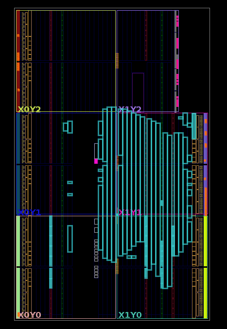
The following is an FPGA floorplan of IBEX demo system in an Artix7 FPGA (default target).