Attention
This document was last updated Nov 25 24 at 21:59
A Coprocessor for the Bresenham Line-Drawing Algorithm
Important
The purpose of this lab is as follows.
To develop a hardware implementation of an algorithm specified as a C function.
The lab assignment covers the following tasks:
Writing RTL code for the C function with simular functionality
Design a hardware interface according to the specification provided
Performing RTL simulation to verify the correctness of the design
Synthesizing the RTL to 45nm standard cells
Making sure that the design meets the clock period constraint
Build a layout for the hardware implementation with pin allocation as specified
Perform post-layout gate-level simulation to demonstrate that the design is still correct
Summarizing the results in a written report
Attention
The due date of this lab is 11 November
The Bresenham Line Drawing Algorithm
In 1962, Jack Elton Bresenham developed a line drawing algorithm to compute which pixels of a raster scan display should be turned on to draw a straight line. The algorithm stands out in that it achieves this task using only integer arithmetic, and addition and substraction. The problem is illustrated in the following figure. Suppose we are drawing a line on a discrete grid from pixel (0,0) to pixel (tx, ty).
The line drawing algorithm needs to decide which pixels should be turned on (grey in the figure). The true mathematical line cuts across fractional pixels, making it challenging to decide when to take, in this example, a vertical step. The solution of Bresenham is to keep an error accumulator that computes how far the center of each pixel remains to the true mathematical line, and to make sure that each pixel that is turned on is never more than half a pixel away from the line.
The Bresenham algorithm is still very popular today in vector-generation algorithms, where you have to create a scalable figure based on a set of vertices. There is a family of ‘Bresenham’ algorithms that are used to draw complex curves and shapes, all of them using simple integer arithmetic.
Because the integer arithmetic used by the Bresenham algorithm, a very efficient hardware implementation is possible. The topic of this lab is to study how a C function can be transformed into a hardware module. In the final project, where you will design a coprocessor for an SoC, this design skill will come in quite handy.
The Bresenham Reference Implementation
The following is a C function that implements the line drawing algorithm. If you are interested in the logic behind the line drawing, refer for example to the Wikipedia article on Bresenham’s Algorithm
 void plotLine(int x1, int y1, int x2, int y2) {
  int dx = abs(x2 - x1);
  int dy = abs(y2 - y1);
  int sx = x1 < x2 ? 1 : -1;
  int sy = y1 < y2 ? 1 : -1;
  int err = dx - dy;

  while (1) {

    printf("%d, %d\n", x1, y1);

    if (x1 == x2 && y1 == y2) break;

    int e2 = 2 * err;

    if (e2 > -dy) {
      err -= dy;
      x1 += sx;
    }

    if (e2 < dx) {
      err += dx;
      y1 += sy;
    }
  }
}
Note the following features of the algorithm.
The algorithm decides on a direction of the line according to each quadrant. This results in the value of
dxanddybeing +1 or -1 to encode the general step direction of a line. For example, in the second quadrant, dx will be negative and dy will be positive.The algorithm uses an error accumulator
errthat keeps track of how far the mathematical line is from the center of a pixel. The error is encoded as an integer value, since the decision on which pixel to turn on next is decided solely by the sign oferr. This is the true brilliance of Bresenham’s Algorithm: by relying only on the sign oferr, the algorithm can scale uperrto a value proportional to the error, rather than the error itself.The algorithm decides between taking a step in only the x-direction, only the y-direction, or in both directions. However, by running small examples, you will see that any set of pixel coordinates will always take a step in either x or else in y, depending on the octant of the line. Only a perfect 45 degree line will cause continuous stepping in both x and y directions, simultaneously.
The algorithm requires signed arithmetic for
dx,dy,sx,sy, anderr. The pixel coordinatesx1,y1,x2,y2can be unsigned.
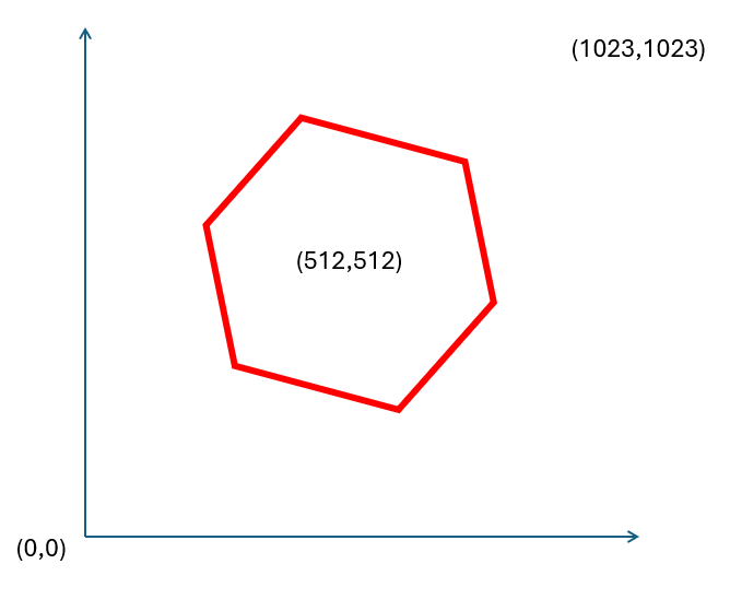
For example, the following testbench generates a (slightly rotated) hexagon. We will use this testbench as the reference.
 int main() {
  plotLine(787, 590, 647, 812);
  plotLine(647, 812, 335, 748);
  plotLine(335, 748, 237, 434);
  plotLine(237, 434, 377, 212);
  plotLine(377, 212, 689, 276);
  plotLine(689, 276, 787, 590);
  return 0;
}
The Bresenham Hardware Interface
Your task is to develop a hardware implementation of the reference implementation of the line drawing algorithm in C. The hardware implementation must be programmable, and must use the following interface.
Name |
Direction |
Function |
|---|---|---|
clk |
Input |
Clock |
resetn |
Input |
Reset, negative-asserted |
D |
Input 10 bit |
Data input to load coordinate values |
ldx1 |
Input |
When asserted, D contains the x1 coordinate |
ldy1 |
Input |
When asserted, D contains the y1 coordinate |
ldx2 |
Input |
When asserted, D contains the x2 coordinate |
ldy2 |
Input |
When asserted, D contains the y2 coordinate |
start |
Input |
When asserted, line drawing starts |
busy |
Output |
When asserted, line drawing in progress |
Xout |
Output 10 bit |
Data output containing the output pixel’s X |
Yout |
Output 10 bit |
Data output containing the output pixel’s Y |
validxy |
Output |
When asserted, (Xout, Yout) is valid |
In addition, the implementation must meet the following performance requirements.
Generate one pixel per clock cycle
Use 45nm standard cell technology
Run at a 3ns clock period (that’s 333MHz!)
Getting Started
Accept the lab2 assignment to obtain the starter files at Github Classroom. This results in a repository with the following subdirectories:
Ccontains a reference implementation in Crtlcontains the template outline of the module you have to designsimcontains a testbench to simulate and verify the RTLsyncontains a synthesis scriptconstraintscontaints the I/O timing constraintslayoutcontains a layout scriptglsimcontaints the post-layout simulation testbenchchipcontains the chip I/O assignment
You will mainly develop code in rtl and in chip.
Step 1: Run the C program
A good first step is to run the C program and play around with the algorithm. Go into the C directory and compile the program. Then, run it. Also, study the algorithm and make sure you understand how the pixel computation loop works.
cd C
gcc vplot.c
./a.out

787, 590
786, 591
786, 592
...
Step 2: Develop the RTL design
You have to design RTL code for the C reference implementation following the interface provided. Give this some careful thought.
module vplot (
   input  logic        clk,
   input  logic        resetn,
   input  logic [9:0]  D,
   input  logic        ldx1,
   input  logic        ldx2,
   input  logic        ldy1,
   input  logic        ldy2,
   input  logic        start,
   output logic [9:0]  Xout,
   output logic [9:0]  Yout,
   output logic        validxy,
   output logic        busy
);
Think of mapping the C function to hardware as two concurrent activities: implementing the control flow of the C program, and implementing the computations done by the C program. The control flow would be implemented using a finite state machine, while the computations would be implemented by a datapath.
Think of mapping the state of the C function to registers. Important state variables are the starting and ending coordinates, the coordinates of the current location, the error, the direction of the line (
sxandsy). By creating registers for these variables and thinking about their update in terms of the C’s program execution, you will systematically develop the hardware design.
Step 3: Perform RTL simulation
You will verify your RTL design using a provided testbench. The
following shows the testbench output when there are errors in the
RTL. Obviously, your RTL design is only complete when you have no more
errors. Make use of the graphical debugger to debug your HDL
code. You can start the XCelium GUI by using make simg instead of
make sim.
cd sim
make

xcelium> source /opt/cadence/XCELIUM2209/tools/xcelium/files/xmsimrc
xcelium> run
ERROR Expected ( 786,  592) Received ( 785,  591)
ERROR Expected ( 785,  593) Received ( 784,  591)
ERROR Expected ( 784,  594) Received ( 784,  592)
ERROR Expected ( 784,  595) Received ( 784,  593)
ERROR Expected ( 783,  596) Received ( 783,  594)
ERROR Expected ( 783,  597) Received ( 782,  594)
ERROR Expected ( 782,  598) Received ( 782,  595)
ERROR Expected ( 781,  599) Received ( 782,  596)
ERROR Expected ( 781,  600) Received ( 782,  597)
ERROR Expected ( 780,  601) Received ( 781,  598)
ERROR Expected ( 779,  602) Received ( 780,  598)
ERROR Expected ( 779,  603) Received ( 780,  599)
ERROR Expected ( 778,  604) Received ( 780,  600)
ERROR Expected ( 778,  605) Received ( 780,  601)
ERROR Expected ( 777,  606) Received ( 779,  602)
ERROR Expected ( 776,  607) Received ( 778,  602)
ERROR Expected ( 776,  608) Received ( 778,  603)
ERROR Expected ( 775,  609) Received ( 778,  604)
ERROR Expected ( 774,  610) Received ( 778,  605)
ERROR Expected ( 774,  611) Received ( 777,  606)
ERROR Expected ( 773,  612) Received ( 776,  606)
ERROR Expected ( 772,  613) Received ( 775,  606)
ERROR Expected ( 772,  614) Received ( 775,  607)
ERROR Expected ( 771,  615) Received ( 775,  608)
ERROR Expected ( 771,  616) Received ( 774,  609)
ERROR Expected ( 770,  617) Received ( 773,  609)
ERROR Expected ( 769,  618) Received ( 773,  610)
ERROR Expected ( 769,  619) Received ( 773,  611)
ERROR Expected ( 768,  620) Received ( 773,  612)
ERROR Expected ( 767,  621) Received ( 772,  613)
ERROR Expected ( 767,  622) Received ( 771,  613)
ERROR Expected ( 766,  623) Received ( 771,  614)
ERROR Expected ( 766,  624) Received ( 771,  615)
Simulation stopped via $stop(1) at time 425 NS + 0
./vplot_tb.sv:129       $stop;
Step 3: Perform RTL synthesis
Once you have a working RTL simulation, you can complete RTL synthesis.
cd syn
make

BASENAME=vplot \
CLOCKPERIOD=3 \
TIMINGPATH=/opt/cadence/libraries/gsclib045_all_v4.7/gsclib045/timing/ \
TIMINGLIB=slow_vdd1v0_basicCells.lib \
genus -f genus_script.tcl
TMPDIR is being set to /tmp/genus_temp_31271_arc-schaumont-class-vm_pschaumont_2HG8MG
Cadence Genus(TM) Synthesis Solution.
...
When synthesis completes, make sure to check the reports for timing and area. You should have no negative slack (for setup timing), and you should have no latches in the netlist. It’s a little more tricky to check your design for latches. The quickest method may be to grep the gate level netlist and look for cells of the ‘TLAT’ type (which are latches).
cd reports
cat vplot_report_timing.rpt
cd ../outputs
grep TLAT vplot_netlist.v
Step 4: Build the chip outline
Before you can implement the layout, you have to build the chip input/output outline.
Create a chip/chip.io file that assigns pins as follows along the chip perimeter.
Along the top, arrange all control signals as well as clk and resetn.
Along the left side, arrange the pins of the D input
Along the right side, arrange the pins of the X and Y output
After you have created the chip I/O, create the layout.
cd layout
make syn
make layout
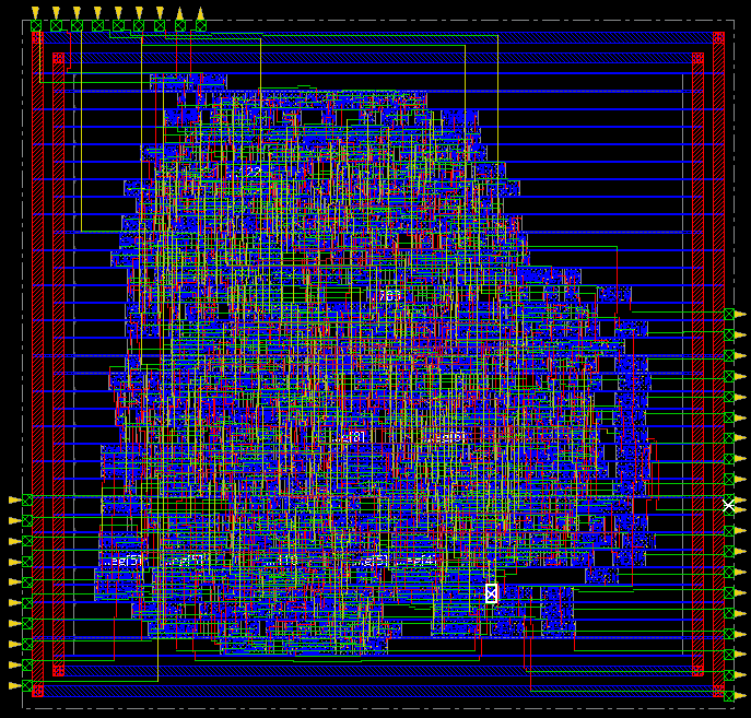
Inside of the innovus tool, you can open up the layout to make a screen shot.
gui_show
If you have a complete design, you should be able to produce something as follows:
Step 5: Perform post-layout gate-level simulation
Your final step is to perform a gate-level timing-accurate simulation of the design post-layout. The design must still be functionall correct.
cd glsim
make
Important
In this lab, steps 3-5 are a minor effort compared to step 1-2. Make sure that you think carefully through your hardware design. Apply the rules of purely synchronous single-clock design, and clearly partition datapath from control (FSM). Also, clearly partition combinational logic (always @* or always_comb) from sequential logic (always @(posedge clk) or always_ff). Your attention to detail in step 2 will pay off in later steps.
Writing your report
Your report should contain the following
A System Verilog Listing of your design
A statement that your design is functionally correct post-synthesis as well as post-layout
A comprehensive performance evaluation, including area, cell counts, post-synthesis timing analysis, post-layout chip area, post-layout timing analysis
A chip layout
Please format your output results and do not cut and paste from the tool output.
Attention
The following are important report requirements.
Use a typesetting tool such as latex or word. Do not submit handwritten scanned reports.
Use a screen capture tool to collect graphics such as layout information. Do not use your smartphone to take a picture from the screen.
Be clear and complete in your report. I am not looking for the correct solution; I am looking to understand your solution. Explain the steps that lead up to a result. The report does not have a minimum length nor a maximum length, as long as it is clear what you did and your answers to questions are complete.
Make sure to update, commit and push the results of your lab to your repository. You do not have to turn in anything on Canvas. All results will be communicated through your github repository.