Attention
This document was last updated Nov 25 24 at 21:59
Timing Analysis
Important
The purpose of this lecture is the following.
To define timing constraints of a synchronous digital circuit
To describe timing analysis of a synchronous digital circuit
To describe the delay modeling techniques used in hardware ASIC
To describe the impact of the environment on timing analysis
To describe the use of a static timing analysis tool
Attention
The following references are relevant background to this lecture.
Chadha, R. and Bhasker, J., “Static Timing Analysis for Nanometer Designs,” Springer-Verlag, 2009. Chapter 2, 3, and 5. https://doi.org/10.1007/978-0-387-93820-2
Attention
The example discussed in this lecture is available on https://github.com/wpi-ece574-f24/ex-sta
Timing Requirements for Synchronous Circuit Operation
Correct timing in synchronous logic generally means that every flip-flop meets its basic timing requirements which include setup and hold timing (for synchronous inputs) and removal and recovery timing (for asynchronous inputs).
Setup, Hold, Recovery, Removal Time
The following figure shows an edge-triggered flip-flop with an asynchronous set input. The synchronous input D is read and stored on the synchronous output Q. Four clock cycles demonstrate the meaning of setup, hold, removal and recovery.
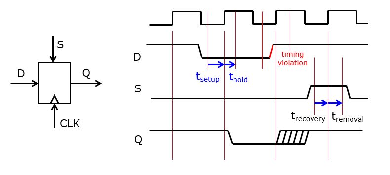
The setup time
 is the duration when a synchronous input
must be stable before a clock edge. The hold time
is the duration when a synchronous input
must be stable before a clock edge. The hold time  is the
duration when a synchronous input must be stable after a clock edge. When a
synchronous input changes during the setup/hold window, a timing
violation occurs which may leave the flip-flop in an undefined state. For
example, the input D changes just before the third clock edge, creating a
timing violation. The flip-flop may remain at 0, or it may switch to 1, or
it may switch to 1 after a long time (e.g. half a clock cycle). Physically,
any of these cases are possible as the flip-flop is in a metastable
state.
is the
duration when a synchronous input must be stable after a clock edge. When a
synchronous input changes during the setup/hold window, a timing
violation occurs which may leave the flip-flop in an undefined state. For
example, the input D changes just before the third clock edge, creating a
timing violation. The flip-flop may remain at 0, or it may switch to 1, or
it may switch to 1 after a long time (e.g. half a clock cycle). Physically,
any of these cases are possible as the flip-flop is in a metastable
state.The recovery time
 is the duration that an asynchronous
that an asynchronous input must be de-asserted before a clock edge, in
order to recover normal synchronous operation. The removal time
is the duration that an asynchronous
that an asynchronous input must be de-asserted before a clock edge, in
order to recover normal synchronous operation. The removal time  is the duration that an asynchronous input must remain asserted
after a clock edge, in order to ensure the asynchronous command has effect.
Just before the fourth clock edge, the asynchronous S input is asserted,
which will force the Q output to take 1 (asserted). The S input remains
asserted longer than
is the duration that an asynchronous input must remain asserted
after a clock edge, in order to ensure the asynchronous command has effect.
Just before the fourth clock edge, the asynchronous S input is asserted,
which will force the Q output to take 1 (asserted). The S input remains
asserted longer than  after the clock edge, thus
ensuring the flip-flop returns to a stable 1.
after the clock edge, thus
ensuring the flip-flop returns to a stable 1.
Stable Operation
Let’s first establish the conditions for a synchronous circuit has correct timing. We will assume only synchronous inputs in the following examples.
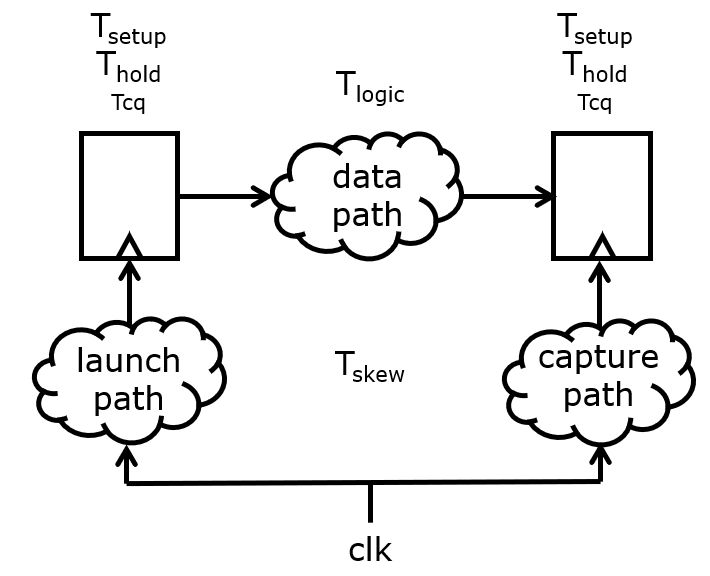
A central clock is distributed to two flip-flops with a data path in
between. The launch path is the route followed by the clock signal
(potentially including clock buffers) up until the clock input of the launch
flip-flop. The capture path is the route followed by the clock signal up
until the clock input of the capture flip-flop. The flip-flops are
characterized by setup time  , hold time
  and
clock-to-q time
and
clock-to-q time  . The latter is the time needed for the
synchronous output Q to be updated after a clock edge. The propagation
delay for the datapath
. The latter is the time needed for the
synchronous output Q to be updated after a clock edge. The propagation
delay for the datapath  is the time needed for the data
path output to be stable after its input is updated. Finally, the launch path
and capture path may result in clock skew between the two flip-flops,
meaning that the clock edge at each flip-flop does not arrive at exactly the
same moment.
is the time needed for the data
path output to be stable after its input is updated. Finally, the launch path
and capture path may result in clock skew between the two flip-flops,
meaning that the clock edge at each flip-flop does not arrive at exactly the
same moment.
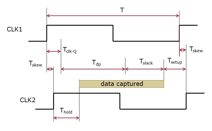
We can now derive conditions towards the
smallest possible clock period  that will ensure stable
circuit operation.
that will ensure stable
circuit operation.
Clock Period Lower Bound
The data arriving at the capture flip flop must be stable before the capture clock edge. The slack is the margin available between the data arrival and the setup boundary at the capture flip-flop.

We want  to be positive, and therefore the following
condition must hold.
to be positive, and therefore the following
condition must hold.

Therefore, the setup time, clk-Q time and skew all potentially reduce
the time available for datapath computations. Note that in this formula,
the sign of  was not flipped when moving over from one
side of the equation to the other. That is because skew relates
to clock uncertainty. In the figure shown above, the skew from CLK1 to
CLK2 actually helps with the minimum allowed clock period. CLK2 is
delayed and therefore gives the datapath a little bit more time to
settle. However, it’s a fallacy to think that this helps our cause; simply
reversing the role of CLK2 and CLK1 in the launch path and the capture path
will make the skew work against the datapath. So, in actual timing analysis,
the skew is modeled as an uncertainty on the clock, and the uncertainty
is counted as a retricting the result.
was not flipped when moving over from one
side of the equation to the other. That is because skew relates
to clock uncertainty. In the figure shown above, the skew from CLK1 to
CLK2 actually helps with the minimum allowed clock period. CLK2 is
delayed and therefore gives the datapath a little bit more time to
settle. However, it’s a fallacy to think that this helps our cause; simply
reversing the role of CLK2 and CLK1 in the launch path and the capture path
will make the skew work against the datapath. So, in actual timing analysis,
the skew is modeled as an uncertainty on the clock, and the uncertainty
is counted as a retricting the result.
Important
The minimum clock period in a synchronous digital circuit is constrained by the setup time of the flip-flops, the clk-Q time of the flip-flops, the slowest datapath, and the clock skew between launch and capture flip-flop.

Clock Skew Upper Bound
Clock skew has to be limited and ideally, for a properly implemented clock distribution circuit, it is as close as possible to zero. However, clock skew has an upperbound too. Data arriving at the capture flip-flop cannot change in the hold time window of the capture flop-flop.

Therefore, positive skew cannot be larger than the time it takes for data to travel from the launch flip-flop through the datapath. If the skew condition is violated, than the capture flip-flop will grab data on the current clock edge rather than the next clock edge. In simulation, this appears as if the circuit skipping is a cycle, and the capture flip-flop has no effect.

When skew is negative, of course, then this condition is easy to meet. It’s also possible to look at this relation in terms of the minimum propagation delay required on a datapath for stable operation.
Important
The minimum propagation delay of a datapath is constrained by the hold time of the flip-flops, the clock skew between launch and capture flip-flop, and the clock-Q time of the flip-flops.

It’s easy to see why the ideal skew must by 0, and not negative. Assume that you have a circuit with feedback, with two flip-flops in the feedback loop. That is, register R2 is updated with a result computed from R1, and register R1 is updated with a result computed from R2. In that case, a positive skew from R1 to R2 will become a negative skew from R2 to R1, and vice versa. The ideal solution is therefore a zero skew.
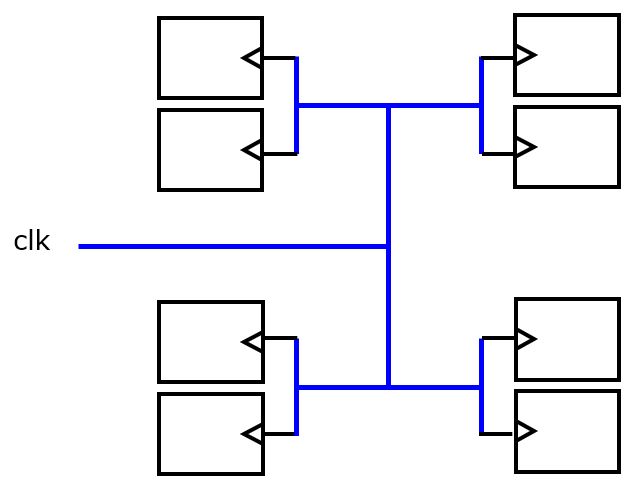
Modern hardware design for ASIC takes the skew problem specifically into account, and will generate a clock tree for a specific circuit. The following figure shows the example of a so-called H-tree which distributes a clock physically to 8 flip-flops in such a way that the skew over all flip-flops becomes close to 0. We will discuss the problem of creating a circuit to distribute the clock signal with low skew in further detail once we discuss layout generation.
Delay Modeling
In order to verify the timing of a complex digital circuit, we must
have a way to quickly compute  . The combinational delay
of a digital circuit depends not only on the (active) logic gates that
evaluate the combinational function, but also on the (passive)
interconnect between the gates. In an ASIC layout, the latter is
defined by the placement of gates on the layout as well as the length
of the interconnect running between individual gates. The fundamental
concepts of Delay Modeling follow from the operation of CMOS logic,
such as the CMOS inverter shown next.
. The combinational delay
of a digital circuit depends not only on the (active) logic gates that
evaluate the combinational function, but also on the (passive)
interconnect between the gates. In an ASIC layout, the latter is
defined by the placement of gates on the layout as well as the length
of the interconnect running between individual gates. The fundamental
concepts of Delay Modeling follow from the operation of CMOS logic,
such as the CMOS inverter shown next.
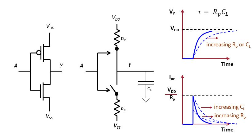
The CMOS inverter uses a p-channel and a n-channel transistor that
will exclusively turned on, depending on the input voltage level at
the common gate A. The equivalent circuit of such a transistor is a
switch controlled by the voltage level on the common gate, as well as
an internal resistor  or
or  . The inverter gate
drives circuit interconnect and other gate inputs which are modeled -
in first order - as a loading capacitor
. The inverter gate
drives circuit interconnect and other gate inputs which are modeled -
in first order - as a loading capacitor  . Hence, when a
CMOS gate switches, it doesn’t make an immediate transition. Instead,
it charges (or discharges) a loading capacitor using an exponential
curve with a time constant propertional to
. Hence, when a
CMOS gate switches, it doesn’t make an immediate transition. Instead,
it charges (or discharges) a loading capacitor using an exponential
curve with a time constant propertional to 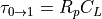 . Because a logic ‘1’ or a logic ‘0’ requires the voltage
to be higher (resp. lower) than a given threshold, it will therefore
take time before the output of a gate has turned from 0 to 1 or vice
versa.
. Because a logic ‘1’ or a logic ‘0’ requires the voltage
to be higher (resp. lower) than a given threshold, it will therefore
take time before the output of a gate has turned from 0 to 1 or vice
versa.
The time constant  can increase because of two factors.
When
or increases, the gate is slower. The
resistance will increase when a weaker gate with smaller transistors
is used, i.e. when the drive strength of the gate decreases. In
addition, when a gate needs to drive a long wire, there is a
non-negligible series resistance that must be added to
or to find the effective resistance.When
increases, the gate is slower. The loading
capacitance is determined by the type and number of gates that are
driven with this gate. The fanout is the number of gates driven,
and the higher the fanout, the slower the gate.
Circuit timing estimators do not directly compute exponential charging and discharging of wires. Instead, they approximate the exponential-shaped waveforms using linear or piecewise linear models. The following shows an example approximation into two popular circuit delay modeling techniques, NLDM (Non Linear Delay Modeling) and CCS (Composite Current Source).
The key difference between an NLDM and CCS model is the level of
sophistication by which the loading capacitance of a gate
is modeled. NLDM assumes a constant loading capacitance, and is
adequate for gate technologies above 90 nm (including the SKY130 PDK
that we will be using for experiments). CCS assumes a variable loading
capacitance, and is used with gate technologies below 90 nm. In the
following discussion, we focus exclusively on NLDM modeling.
NLDM Delay Modeling
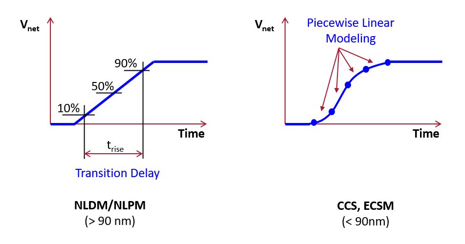
Assume an inverter circuit that drives several other gates. The NLDM model can capture delays in this circuit following the waveforms shown below the circuit.
Each transition is modeled with a given steepness or slew rate. The slew rate, which is typically measured as the time between the 10% and 90% of the signal’s transition voltage, is a first order approximation of the non-linear (exponential) charging/discharging of loading capacitance. Slew rate is modeled in terms of a transition delay. Rather than expressing the steepness of the transition, we capture the time of the transition. The propagation delay of a gate is measured as the response time between an input and a corresponding output, measured as the time between the halfway points of the transition at the input and at the output.
Each input on the network represents an equivalent loading capacitance. On a high-fanout net, many inputs are connected in parallel and thus the loading capacitance rises.
The delay computation tool now has to compute the propagation delay of every cell, as well as the transition delay for every output. The delay computation tool distinguishes rising transitions from falling transitions, and each of these transitions may take a different transition time (on a net) or a different propagation delay (on a cell).
The objective of the delay computation tool is to determine the propagation delay of every gate, as well as the transition time for every output. The propagation delay of a gate depends on the loading capacitance of the gate output, and the transition time at the input. Similarly, the transition time of an output depends on the loading capacitance of the gate output, and the transition time at the input.
When a gate has multiple inputs, there can be multiple factors for the propagation delay and the transition time of the output. The delay computation tool will consider all of them, and then select the worst possible one to reflect the propagation and transition delay of an output. The causal dependence between the input and the output of a gate in terms of delay is called a timing arc. Thus, you can imagine each gate pin as a node in a graph, and the timing arcs as the edges of that graph. Then, the delay computation of the overall circuit can be expressed in terms of finding the slowest path in that graph. Initially, most of the propagation delays and transition delays are unknown, except for those at the input. Then, the delay computation tool starts resolving all the unknowns using a per-gate lookup table, until all delays are known. Finally, the delay of the overall circuit can be determined.
Interconnect Delay Modeling
Delay is also affected by interconnect. The basic delay model of a wire accounts for its resistance and capacitance to ground, which are both proportional to the wire length.
The circuit delay through a wire modeled using an equivalent resistor
 and a capacitor
  is given by the Elmore delay,
which sets the delay at
is given by the Elmore delay,
which sets the delay at  . To account for the distributed
(rather than lumped) nature of wire resistance and wire capacitance,
the elmore delay of a wire is rather
. To account for the distributed
(rather than lumped) nature of wire resistance and wire capacitance,
the elmore delay of a wire is rather  . Hence, the total
delay experienced by a signal edge traveling through the circuit below
is
. Hence, the total
delay experienced by a signal edge traveling through the circuit below
is 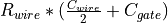 .
.
Interconnect delay is introduced in the delay estimation through two mechanisms: through a wire load model or through parasitics modeling.
Wire Load Models
In advanced technology nodes, wire delay is dominating the delay of the overall circuit. Delay computation tools deal with the delay of wires by estimating the length of the wire. The length of a wire implies an equivalent resistance and capacitance for the wire, and thus, a delay. The loading capacitance is also affecting the transition delay of the gate that drives the wire.
As long as the circuit is not physically constructed into a layout, the length of the wires and the metal layers used for each wire, is not yet known. This creates a chicken-and-egg problem, since without known the precise delays, it’s not possible to accurately size the circuit and select the proper drive strength for each gate. To get around this problem, delay computation tools (and synthesis tools) use a wire load model, an initial estimate of the resistance and capacitance of each wire based on high level circuit factors such as fanout and circuit area.
When the detailed layout of a circuit is known, the wire load model is replaced with more precise estimates for each wire in terms of resistance and capacitance. Thus, as we add more design details to the implementation, the timing estimates computed by the delay computation tool will be more precise. Typically, you will find that the timing of the circuit worsens after layout. However, it should not become so much worst that the post-layout design introduces a significant amount of timing violations. If that would occur, it could indicate that the wire load model that was chosen initially at synthesis, as not a good estimate of the actual circuit area and layout.
The Liberty Format
The delay information of a gate is stored in a specific(human-readable) format called the Liberty Format. Originally devised by Synopsys, the Liberty Format is now an open standard (http://www.opensourceliberty.org/) that is shared by other EDA vendors and cell library providers.
Attention
The Liberty files (or lib files for short) of the 130nm
high-density standard cells are stored under
/opt/skywater/libraries/sky130_fd_sc_hd/latest/timing/. There
are multiple lib files in that directory, corresponding to
different operating corners (temperature, voltage, process).
The Liberty files of CDS45 standard cells are stored under
/opt/cadence/libraries/gsclib045_all_v4.7/gsclib045/timing/. Similarly,
the different lib files in that directory correspond to different
operating corners.
For every gate in the library, the .lib file will capture the load model (the input capacitance of each gate) as well as the drive model (the gate delay and output transition delay). As an example, let’s look at the drive-strength-1 AND2 gate of the CDS45 library. The model is slightly shortened by removing information not related to timing, such as power.
cell (AND2X1) {
  area : 1.368;
  pin (Y) {
    direction : "output";
    function : "(A B)";
    max_capacitance : 0.25;
    timing () {
      related_pin : "A";
      timing_sense : positive_unate;
      timing_type : combinational;
      cell_rise (delay_template_2x2) {
        index_1 ("0.008, 0.28");
        index_2 ("0.01, 0.25");
        values ( \
          "0.221347, 2.96281", \
          "0.349336, 3.09097" \
        );
      }
      rise_transition (delay_template_2x2) {
        index_1 ("0.008, 0.28");
        index_2 ("0.01, 0.25");
        values ( \
          "0.220913, 5.14177", \
          "0.22198, 5.14177" \
        );
      }
      cell_fall (delay_template_2x2) {
        index_1 ("0.008, 0.28");
        index_2 ("0.01, 0.25");
        values ( \
          "0.18609, 3.40759", \
          "0.309193, 3.53088" \
        );
      }
      fall_transition (delay_template_2x2) {
        index_1 ("0.008, 0.28");
        index_2 ("0.01, 0.25");
        values ( \
          "0.259895, 6.18195", \
          "0.260511, 6.18195" \
        );
      }
    }
    timing () {
      related_pin : "B";
      timing_sense : positive_unate;
      timing_type : combinational;
      cell_rise (delay_template_2x2) {
        index_1 ("0.008, 0.28");
        index_2 ("0.01, 0.25");
        values ( \
          "0.230092, 2.97154", \
          "0.366278, 3.10769" \
        );
      }
      rise_transition (delay_template_2x2) {
        index_1 ("0.008, 0.28");
        index_2 ("0.01, 0.25");
        values ( \
          "0.220922, 5.14177", \
          "0.221819, 5.14177" \
        );
      }
      cell_fall (delay_template_2x2) {
        index_1 ("0.008, 0.28");
        index_2 ("0.01, 0.25");
        values ( \
          "0.190622, 3.41312", \
          "0.316799, 3.53945" \
        );
      }
      fall_transition (delay_template_2x2) {
        index_1 ("0.008, 0.28");
        index_2 ("0.01, 0.25");
        values ( \
          "0.260612, 6.18249", \
          "0.261192, 6.18251" \
        );
      }
    }
  pin (A) {
    direction : "input";
    max_transition : 0.28;
    capacitance : 0.000205583;
    rise_capacitance : 0.000205583;
    rise_capacitance_range (0.000202183, 0.000210011);
    fall_capacitance : 0.000164011;
    fall_capacitance_range (0.000143976, 0.0001853);
  }
  pin (B) {
    direction : "input";
    max_transition : 0.28;
    capacitance : 0.000208516;
    rise_capacitance : 0.000208516;
    rise_capacitance_range (0.000205733, 0.000210818);
    fall_capacitance : 0.000186718;
    fall_capacitance_range (0.000182961, 0.000191844);
  }
}
This model captures information related to each pin of the gate:
A, B, and Y. The input pin models are the shortest. The
model encodes input capacitance for rising and falling transitions
separately. It also capture the capacitance range which is needed
for more advanced CCS based delay calculations. The max_transition
attribute is a constraint and represents the slowest transition that
is acceptable for the given cell characterization.
The output pin description is more sophisticated and states the
function (A B) and several timing blocks. Each timing block
encodes a timing arc, and there is a timing block for changes related
to the A input as well as changes related to the B input. The
propagation delay for the gate is encoded as the
cell_fall/cell_rise to capture delay from changes at the
corresponding input. The transition delay for the output is encoded as
fall_transition/rise_transition to capture output transition
time stemming from changes at the corresponding input. Each timing arc
has a unateness, which indicate the direction of the output
transition in function of the input transition. Positive unateness
means the output rises when the input rises, and negative unateness
means the output falls when the input rises. An output pin can also be
non-unate, when there is no logic connection between input and output
transition. For example, the Q output on a flip-flop is non-unate with
respect to the clock input signal.
The delays are encoded in lookup tables. For example, the lookup table
delay_template_2x2 is used to describe the propagation delay for a
rising output triggered from input B:
timing () {
  related_pin : "B";
  timing_sense : positive_unate;
  timing_type : combinational;
  cell_rise (delay_template_2x2) {
    index_1 ("0.008, 0.28");
    index_2 ("0.01, 0.25");
    values ( \
      "0.230092, 2.97154", \
      "0.366278, 3.10769" \
    );
  }
  ...
These encoding used for these lookup tables is stored in the .lib file
as well. For example, for delay_template_2x2 we find:
lu_table_template (delay_template_2x2) {
  variable_1 : input_net_transition;
  variable_2 : total_output_net_capacitance;
  index_1 ("0.008, 0.28");
  index_2 ("0.01, 0.3");
}
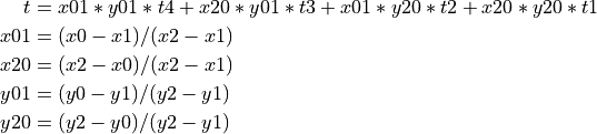
Thus, the first index of cell_rise represents the input transition
delay, and the second index of cell_rise represents the output net
capacitance. The transition delay table for cell_rise is thus
encoded as follows. (index1, index2) map to (row, column).
cell_rise
(x1) 0.01
(x2) 0.3
(y1) 0.008
(t1) 0.230092
(t2) 2.97154
(y2) 0.28
(t3) 0.366278
(t4) 3.10769
Using this table, the timing simulator can determine the right gate
propagation delay from a given capacitive load and a given input
transition. For example, if the input transition (on B) is 0.28ns
and the capacitive load at the output is 0.01 fF, then the gate
propagation delay for a rising transition is 0.366278ns. Then the
index value cannot be directly matched (to either input transition or
output capacitance), the output propagation delay will be found using
linear interpolation. For the following table:
Standard Delay Format
When additional design information becomes available (such as the fanout and type of gates used after synthesis, or the exact topology of interconnect after layout), the delay estimates of gates and wires can be refined. The standard delay format (sdf) is a data format that is used by synthesis and layout tools to provide such updated delay information. The data provided through sdf can override the delays listed in the lib file. Standard delay format can be used, for example, to initialize a gate-level timing simulation. The library provides a functional view of the gates in Verilog, and the SDF captures the delay effects of the gate-level netlist. Keep in mind that typical 4-value HDL simulation (0,1,X,Z) cannot simulate slew or transition delay.
The following is an example of an entry in an sdf file, produced by
the synthesis tool. It describes the delays of a gate g828__3680.
(CELL
   (CELLTYPE "ADDFX1")
   (INSTANCE g828__3680)
   (DELAY
      (ABSOLUTE
        (PORT A (::0.000))
        (PORT B (::0.000))
        (PORT CI (::0.000))
        (IOPATH CI CO (::0.186) (::0.172))
        (IOPATH A CO (::0.200) (::0.173))
        (IOPATH B CO (::0.198) (::0.173))
        (IOPATH CI S (::0.286) (::0.268))
        (IOPATH A S (::0.281) (::0.300))
        (IOPATH B S (::0.291) (::0.294))
      )
   )
)
(CELLTYPE "ADDFX1")specifies the type of the cell, which is “ADDFX1” in this case.(INSTANCE g828__3680)specifies the instance name of the cell, which is “g828__3680.”(DELAY ...)defines the delay characteristics of the cell instance.(ABSOLUTE ...)indicates that the delay values provided are absolute delays.(PORT A (::0.000))specifies that the input port “A” has an absolute delay of 0.000 time units. Similar specifications hold forBandCI.(IOPATH CI CO (::0.186) (::0.172))defines an input-to-output path from “CI” to “CO” with an absolute delay of 0.186 time units and a slew (transition) delay of 0.172 time units. Similar specifications hold for other IO paths of the gate.
Static Timing Analysis
We are now ready to perform timing analysis of a complete circuit. Through delay modeling, we can annotate each gate (and possibly wire) with a given propagation delay. Now, given an arbitrarily complex circuit, we would like to verify if the setup delay constraints of flip-flops in the design are met.
First, we demonstrate how slack can be computed for any node in an arbtitrary combinational circuit. Next, we then expand this method to the static timing analysis algorithm to verify the setup/hold time of every flip-flop in the circuit, as well as the arrival time of every system output.
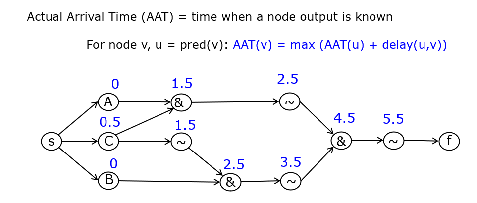
Actual Arrival Time in a combinational circuit
Using a straightforward graph algorithm, the propagation delay of a
network of combinational gates is computed as follows. We use the
following example as an illustration. A three-input network has a
propagation delay of 1 ns for every gate. All inputs except C are
available at the start of the clock cycle, while C is only ready
after 0.5ns. Such an input delay is a typical constraint encountered
in actual timing analysis calculations, as we will illustrate later.
To compute the propagation delay of this circuit, we need to determine the actual arrival time (AAT), the time when output Q is available. All gates are mapped as nodes in a graph, and interconnections are mapped as edges. Inputs and outputs map to their own node. Each node is then annotated with a propagation delay, and the AAT is compute from inputs to outputs, by identifying the latest time each node output is available.
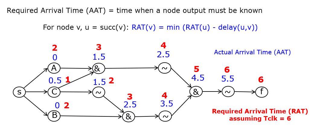
Next, we compute the required arrival time (RAT) for each node in the graph under the assumption of a given clock period. While AAT is computed from input to output, the RAT is computed from output to inputs, each time identifying the latest possible time that a node input must be ready in order to meet the overall RAT.
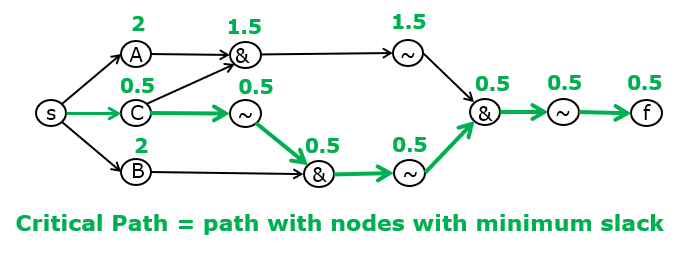
Finally, the slack for the circuit output, and every other node in the graph, is the difference between the RAT and the AAT. The slack must always be positive. A negative slack (for any node in the graph) indicates a timing violation and thus a circuit that does not meet its timing constraints. Also, the critical path in the graph becomes visible by highlighting all nodes with minimum slack. In the case of the example, we see that the critical path runs through input C (the slowest input) and the path that cross a maximumm overall gate delay.
Applying static timing analysis in sequential logic
The perform static timing analysis on sequential logic, the slack computation algorithm is applied to every block of combinational logic in a given module. There are four possible paths in such a circuit. These four paths enumerate the four possible paths between two kinds of inputs (module input and register output) and two kinds of output (module output and register input). The four paths are:
Combinational logic from module input to module output
Combinational logic from module input to register input
Combinational logic from register output to module output
Combinational logic from register output to register input
We compute the slack for each of these paths, and verify that each slack is positive. Static analysis tools use the term path group to mark such similar paths. In designs with multiple clocks, there can be more than four possible path groups, and the static timing analysis tool will verify to slack in every group.
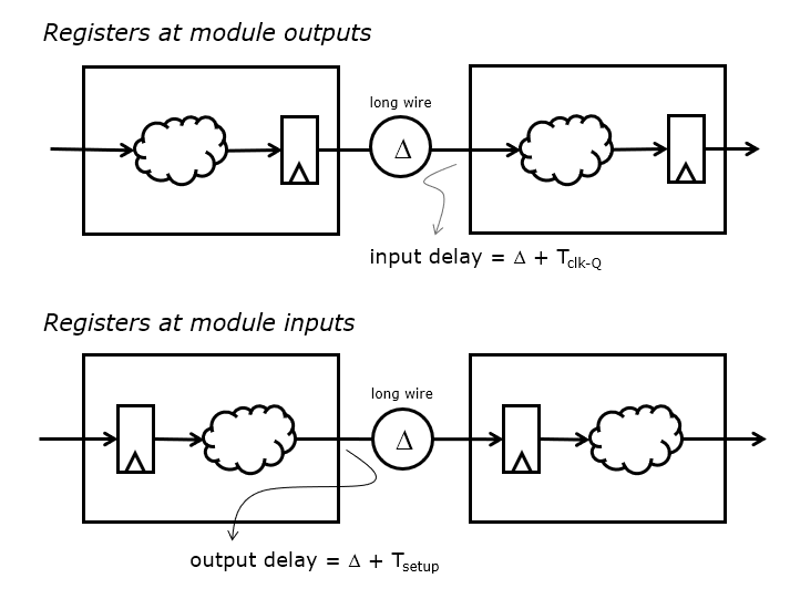
Input and Output Delay
In principle, the required arrival time is equal to the chosen clock period at which the tming analysis is performed. However, there are practical arguments to verify against a tighter constraint, in particular because the module inputs and module outputs can introduce their own timing constraint.
Each input can be associated with an input delay, the time after the clock edge at which the input is valid. Furthermore, each output can be associated with an output delay, the time before the clock edge at which the output must be available. The ideal input delay, as well as the ideal output delay, is zero, meaning that the entire clock period can be used for combinational computation. However, registers cannot meet that constraint. Every register has a non-zero clk-Q time, which determines the ‘input delay’ for the paths starting at a register output. Also, every register has a positive setup time, which determines the ‘output delay’ for paths ending at a register input.
In addition, external interfaces (such as the connections to memory modules) can introduce additional input/output constraints. The following example shows how one could select an input delay in an interconnect strategy that puts registers at the output. Below that, how one coudl select an output delay constraint in an interconnect strategy that puts registers at the input.
Timing Analysis with Tempus
Refer to the materials posted on Canvas (Timing Paths and SDC Constraints)
Example
We will discuss static timing analysis on the following multiply-accumulate example. Notice that this module has all four types of timing paths we discussed above: input to output, input to register, register to register and register to output.
module mac(
    input logic [7:0] x1,
    input logic [7:0] x2,
    output logic [9:0] y,
    output logic [9:0] m,
    input logic reset,
    input logic clk
);

   logic [9:0] y_next;
   logic [15:0] m16;

   always_ff @(posedge clk)
       if (reset)
         y <= 10'b0;
       else
         y <= y_next;

   always_comb
     begin
        m16 = x1 * x2;
        m = m16[15:6];
        y_next = y + m;
     end

endmodule
First, perform RTL synthesis in the syn directory.
cd syn
make
The resulting module is implemented using 163 standard cells for a 4
ns clock constraint. The synthesis timing report states a slack of
633ps, with the critical path running from the input (x2[0]) to
the accumulator register msb (y[9]). The critical path of the
design thus includes the multiply-accumulate operation, and within
those operations the path includes the complete carry chain from LSB
to MSB.
#---------------------------------------------------------------------------------------------------------
#          Timing Point           Flags    Arc   Edge   Cell     Fanout Load Trans Delay Arrival Instance
#                                                                       (fF)  (ps)  (ps)   (ps)  Location
#---------------------------------------------------------------------------------------------------------
  x2[0]                           -       -      R     (arrival)      7  2.6     0     0       0    (-,-)
  mul_21_11_g847__4319/Y          -       A->Y   F     NAND2X1        2  0.8    76    61      61    (-,-)
  mul_21_11_g817__5107/Y          -       A->Y   R     NOR2X1         2  1.2    84   100     160    (-,-)
  mul_21_11_g806__4733/Y          -       B0->Y  F     AOI21X1        1  0.5    77    69     230    (-,-)
  mul_21_11_cdnfadd_003_0__2883/S -       CI->S  R     ADDFX1         2  0.8    46   307     537    (-,-)
  mul_21_11_g802__1881/Y          -       A1->Y  F     OAI221X1       1  0.4   154   166     703    (-,-)
  mul_21_11_g798__7098/Y          -       A1->Y  R     AOI22X1        2  0.8    87   157     860    (-,-)
  mul_21_11_g796__8246/Y          -       C->Y   F     NOR3BX1        1  0.4    43    72     931    (-,-)
  mul_21_11_g794__1705/Y          -       A1->Y  R     OAI22X1        1  0.8   100    87    1018    (-,-)
  mul_21_11_g793__2802/CO         -       B->CO  R     ADDFX1         1  0.6    39   230    1249    (-,-)
  mul_21_11_g792__1617/CO         -       CI->CO R     ADDFX1         1  0.6    39   186    1435    (-,-)
  mul_21_11_g791__3680/CO         -       CI->CO R     ADDFX1         1  0.6    39   186    1621    (-,-)
  mul_21_11_g790__6783/CO         -       CI->CO R     ADDFX1         1  0.6    39   186    1807    (-,-)
  mul_21_11_g789__5526/CO         -       CI->CO R     ADDFX1         1  0.6    39   186    1993    (-,-)
  mul_21_11_g788__8428/CO         -       CI->CO R     ADDFX1         1  0.6    39   186    2179    (-,-)
  mul_21_11_g787__4319/CO         -       CI->CO R     ADDFX1         1  0.6    39   186    2365    (-,-)
  mul_21_11_g786__6260/CO         -       CI->CO R     ADDFX1         1  0.6    39   186    2551    (-,-)
  mul_21_11_g785__5107/S          -       CI->S  F     ADDFX1         2  0.7    45   271    2822    (-,-)
  g707__4319/CO                   -       B->CO  F     ADDFX1         1  0.4    37   172    2994    (-,-)
  g705__5107/Y                    -       B->Y   R     XNOR2X1        1  0.2    22   163    3157    (-,-)
  g703__2398/Y                    -       AN->Y  R     NOR2BX1        1  0.3    39    86    3243    (-,-)
  y_reg[9]/D                      <<<     -      R     DFFHQX1        1    -     -     0    3243    (-,-)
#---------------------------------------------------------------------------------------------------------
For a better insight into the timing behavior of the module, we run
the timing analysis again under sta.
cd ta
make
The static timing analysis makes use of the following timing analysis script. The following indicate particular activities.
The script inputs are the gate-level netlist, the standard cell library, and the constraint file as well as the SDF generated by the synthesis. Thus, the STA results from this run may not be identical to those produced by the synthesis because the constraints/sdf is not identical.
The script produces three files. The first file,
late.rptshows the three longest paths in the system as they pertain to register setup tests. The second file,early.rptshows the three longest paths in the system as they pertain to register hold checks. The third file,allpaths.rpt, shows a summary of the longest path starting at each input, output, register input and register output. This third file gives an understanding how the worst case path (fromx2[0]toy[9]) relates to other slow paths in the module.The script uses Tempus commands; consult the Tempus command reference manual (on Cadence support) for variations of these commands. Some of them, such as
report_timing, support many variations and are worth exploring.
read_lib /opt/cadence/libraries/gsclib045_all_v4.7/gsclib045/timing/slow_vdd1v0_basicCells.lib

read_verilog ../syn/outputs/mac_netlist.v
set_top_module mac

read_sdc ../syn/outputs/mac_constraints.sdc
read_sdf ../syn/outputs/mac_delays.sdf

report_timing -late -max_paths 3 > late.rpt
report_timing -early -max_paths 3 > early.rpt

report_timing  -from [all_inputs] -to [all_outputs] -max_paths 12 -path_type summary  > allpaths.rpt
report_timing  -from [all_inputs] -to [all_registers] -max_paths 12 -path_type summary  >> allpaths.rpt
report_timing  -from [all_registers] -to [all_registers] -max_paths 12 -path_type summary >> allpaths.rpt
report_timing  -from [all_registers] -to [all_outputs] -max_paths 12 -path_type summary >> allpaths.rpt
exit
First, let’s look at the worst path from late.rpt. That path turns
out to be worse than the path reported by the synthesis tool although
it’s quite close. The differences are cause by the use of SDF.
Path 1: MET Setup Check with Pin y_reg[9]/CK
Endpoint:   y_reg[9]/D (^) checked with  leading edge of 'clk'
Beginpoint: x2[0]      (^) triggered by  leading edge of 'clk'
Path Groups: {clk}
Other End Arrival Time          0.000
- Setup                         0.124
+ Phase Shift                   4.000
= Required Time                 3.876
- Arrival Time                  3.291
= Slack Time                    0.585
     Clock Rise Edge                      0.000
     + Input Delay                        0.000
     = Beginpoint Arrival Time            0.000
      -------------------------------------------------------------------------------
      Instance                       Arc           Cell      Delay  Arrival  Required
                                                                    Time     Time
      -------------------------------------------------------------------------------
      -                              x2[0] ^       -         -      0.000    0.585
      mul_21_11_g847__4319           A ^ -> Y v    NAND2X1   0.061  0.061    0.646
      mul_21_11_g817__5107           A v -> Y ^    NOR2X1    0.100  0.161    0.746
      mul_21_11_g806__4733           B0 ^ -> Y v   AOI21X1   0.069  0.230    0.815
      mul_21_11_cdnfadd_003_0__2883  CI v -> S ^   ADDFX1    0.307  0.537    1.122
      mul_21_11_g802__1881           A1 ^ -> Y v   OAI221X1  0.166  0.703    1.288
      mul_21_11_g798__7098           A1 v -> Y ^   AOI22X1   0.157  0.860    1.445
      mul_21_11_g796__8246           C ^ -> Y v    NOR3BX1   0.072  0.932    1.517
      mul_21_11_g794__1705           A1 v -> Y ^   OAI22X1   0.087  1.019    1.604
      mul_21_11_g793__2802           B ^ -> CO ^   ADDFX1    0.230  1.249    1.834
      mul_21_11_g792__1617           CI ^ -> CO ^  ADDFX1    0.186  1.435    2.020
      mul_21_11_g791__3680           CI ^ -> S ^   ADDFX1    0.290  1.725    2.310
      g725__1881                     B ^ -> CO ^   ADDFX1    0.203  1.928    2.513
      g722__7098                     CI ^ -> CO ^  ADDFX1    0.186  2.114    2.699
      g719__5122                     CI ^ -> CO ^  ADDFX1    0.186  2.300    2.885
      g716__2802                     CI ^ -> CO ^  ADDFX1    0.186  2.486    3.071
      g713__3680                     CI ^ -> CO ^  ADDFX1    0.186  2.672    3.257
      g710__5526                     CI ^ -> CO ^  ADDFX1    0.186  2.858    3.443
      g707__4319                     CI ^ -> CO ^  ADDFX1    0.184  3.042    3.627
      g705__5107                     B ^ -> Y ^    XNOR2X1   0.163  3.205    3.790
      g703__2398                     AN ^ -> Y ^   NOR2BX1   0.086  3.291    3.876
      y_reg[9]                       D ^           DFFHQX1   0.000  3.291    3.876
      -------------------------------------------------------------------------------
Next, look at the fastest path with respect to hold time in
early.rpt. This path runs from reset to a register input. The
overall module uses syncrhonous reset, so this reset signal is a
simple system input. Because the system constraint uses an input delay
of 0, the STA assumes that reset can change directly after the upgoing
clock edge, thereby potentially affecting y_reg[7]. However, as
the report shows, there is no hold time violation.
Path 1: MET Hold Check with Pin y_reg[7]/CK
Endpoint:   y_reg[7]/D (v) checked with  leading edge of 'clk'
Beginpoint: reset      (^) triggered by  leading edge of 'clk'
Path Groups: {clk}
Other End Arrival Time          0.000
+ Hold                          0.006
+ Phase Shift                   0.000
= Required Time                 0.006
  Arrival Time                  0.020
  Slack Time                    0.014
     Clock Rise Edge                      0.000
     + Input Delay                        0.000
     = Beginpoint Arrival Time            0.000
      ---------------------------------------------------------
      Instance    Arc         Cell     Delay  Arrival  Required
                                              Time     Time
      ---------------------------------------------------------
      -           reset ^     -        -      0.000    -0.014
      g709__8428  B ^ -> Y v  NOR2BX1  0.020  0.020    0.006
      y_reg[7]    D v         DFFHQX1  0.000  0.020    0.006
      ---------------------------------------------------------
Finally, look at the path summary of the overall module in
allpath.rpt. This results show that the slack is minimal indeed
for the input-to-register path. Note also the significant variation
of the slack within a path group (e.g. input-to-register) as well as
between apth groups. In this case, the x2[0 to y_reg[9] path
is so much longer than anything else, that it dominates the
delay. Hence, any timing optimization on this module should start by
considering that specific part of the design. However, in other case,
other parts of the design may be equally slow so that the critical
path tends to jump around as soon as we start making small
changes/optimzations. The use of STA (and tempus, in particular) can
help us understand how design changes can affect the critical path. In
the quiz, you will explore this aspect further.
#  Command:           report_timing  -from [all_inputs] -to [all_outputs] -max_paths 12 -path_type summary  > allpaths.rpt
      --------------------------------------------------------------------------------------------------------------------------------------
       Path No.   Begin Point         End Point            Slack      Arrival        Required   Phase                  Other Phase
      --------------------------------------------------------------------------------------------------------------------------------------
      1          x2[0] ^             m[8] ^               1.159      2.841          4.000      clk(D)(P) *            clk(C)(P)
      2          x2[0] ^             m[9] ^               1.265      2.735          4.000      clk(D)(P) *            clk(C)(P)
      3          x2[0] ^             m[7] ^               1.345      2.655          4.000      clk(D)(P) *            clk(C)(P)
      4          x2[0] ^             m[6] ^               1.531      2.469          4.000      clk(D)(P) *            clk(C)(P)
      5          x2[0] ^             m[5] ^               1.717      2.283          4.000      clk(D)(P) *            clk(C)(P)
      6          x2[0] ^             m[4] ^               1.903      2.097          4.000      clk(D)(P) *            clk(C)(P)
      7          x2[0] ^             m[3] ^               2.089      1.911          4.000      clk(D)(P) *            clk(C)(P)
      8          x2[0] ^             m[2] ^               2.275      1.725          4.000      clk(D)(P) *            clk(C)(P)
      9          x2[0] ^             m[1] ^               2.463      1.537          4.000      clk(D)(P) *            clk(C)(P)
      10         x2[3] ^             m[0] v               2.647      1.353          4.000      clk(D)(P) *            clk(C)(P)
      --------------------------------------------------------------------------------------------------------------------------------------

#  Command:           report_timing  -from [all_inputs] -to [all_registers] -max_paths 12 -path_type summary  >> allpaths.rpt
      --------------------------------------------------------------------------------------------------------------------------------------
       Path No.   Begin Point         End Point            Slack      Arrival        Required   Phase                  Other Phase
      --------------------------------------------------------------------------------------------------------------------------------------
      1          x2[0] ^             y_reg[9]/D ^         0.585      3.291          3.876      clk(D)(P) *            clk(C)(P)
      2          x2[0] ^             y_reg[8]/D ^         0.643      3.233          3.876      clk(D)(P) *            clk(C)(P)
      3          x2[0] ^             y_reg[7]/D ^         0.829      3.047          3.876      clk(D)(P) *            clk(C)(P)
      4          x2[0] ^             y_reg[6]/D ^         1.015      2.861          3.876      clk(D)(P) *            clk(C)(P)
      5          x2[0] ^             y_reg[5]/D ^         1.201      2.675          3.876      clk(D)(P) *            clk(C)(P)
      6          x2[0] ^             y_reg[4]/D ^         1.387      2.489          3.876      clk(D)(P) *            clk(C)(P)
      7          x2[0] ^             y_reg[3]/D ^         1.573      2.303          3.876      clk(D)(P) *            clk(C)(P)
      8          x2[0] ^             y_reg[2]/D ^         1.767      2.109          3.876      clk(D)(P) *            clk(C)(P)
      9          x2[0] ^             y_reg[1]/D ^         1.964      1.912          3.876      clk(D)(P) *            clk(C)(P)
      10         x2[3] ^             y_reg[0]/D ^         2.348      1.511          3.859      clk(D)(P) *            clk(C)(P)
      --------------------------------------------------------------------------------------------------------------------------------------

#  Command:           report_timing  -from [all_registers] -to [all_registers] -max_paths 12 -path_type summary >> allpaths.rpt
      --------------------------------------------------------------------------------------------------------------------------------------
       Path No.   Begin Point         End Point            Slack      Arrival        Required   Phase                  Other Phase
      --------------------------------------------------------------------------------------------------------------------------------------
      1          y_reg[0]/Q ^        y_reg[9]/D ^         1.821      2.055          3.876      clk(D)(P) *            clk(C)(P)
      2          y_reg[0]/Q ^        y_reg[8]/D ^         1.879      1.997          3.876      clk(D)(P) *            clk(C)(P)
      3          y_reg[0]/Q ^        y_reg[7]/D ^         2.065      1.811          3.876      clk(D)(P) *            clk(C)(P)
      4          y_reg[0]/Q ^        y_reg[6]/D ^         2.251      1.625          3.876      clk(D)(P) *            clk(C)(P)
      5          y_reg[0]/Q ^        y_reg[5]/D ^         2.437      1.439          3.876      clk(D)(P) *            clk(C)(P)
      6          y_reg[0]/Q ^        y_reg[4]/D ^         2.623      1.253          3.876      clk(D)(P) *            clk(C)(P)
      7          y_reg[0]/Q ^        y_reg[3]/D ^         2.809      1.067          3.876      clk(D)(P) *            clk(C)(P)
      8          y_reg[0]/Q ^        y_reg[2]/D ^         2.995      0.881          3.876      clk(D)(P) *            clk(C)(P)
      9          y_reg[0]/Q ^        y_reg[1]/D ^         3.187      0.689          3.876      clk(D)(P) *            clk(C)(P)
      10         y_reg[0]/Q v        y_reg[0]/D ^         3.506      0.353          3.859      clk(D)(P) *            clk(C)(P)
      --------------------------------------------------------------------------------------------------------------------------------------

#  Command:           report_timing  -from [all_registers] -to [all_outputs] -max_paths 12 -path_type summary >> allpaths.rpt
      --------------------------------------------------------------------------------------------------------------------------------------
       Path No.   Begin Point         End Point            Slack      Arrival        Required   Phase                  Other Phase
      --------------------------------------------------------------------------------------------------------------------------------------
      1          y_reg[1]/Q v        y[1] v               3.798      0.202          4.000      clk(D)(P) *            clk(C)(P)
      2          y_reg[2]/Q v        y[2] v               3.798      0.202          4.000      clk(D)(P) *            clk(C)(P)
      3          y_reg[3]/Q v        y[3] v               3.798      0.202          4.000      clk(D)(P) *            clk(C)(P)
      4          y_reg[4]/Q v        y[4] v               3.798      0.202          4.000      clk(D)(P) *            clk(C)(P)
      5          y_reg[5]/Q v        y[5] v               3.798      0.202          4.000      clk(D)(P) *            clk(C)(P)
      6          y_reg[6]/Q v        y[6] v               3.798      0.202          4.000      clk(D)(P) *            clk(C)(P)
      7          y_reg[7]/Q v        y[7] v               3.798      0.202          4.000      clk(D)(P) *            clk(C)(P)
      8          y_reg[8]/Q v        y[8] v               3.798      0.202          4.000      clk(D)(P) *            clk(C)(P)
      9          y_reg[0]/Q v        y[0] v               3.804      0.196          4.000      clk(D)(P) *            clk(C)(P)
      10         y_reg[9]/Q v        y[9] v               3.806      0.194          4.000      clk(D)(P) *            clk(C)(P)
      --------------------------------------------------------------------------------------------------------------------------------------