Signal Sampling and Reconstruction
Contents
Important
The purpose of this lecture is as follows.
To review the essentials of signal sampling (Dirac Impulse, DTFT)
To review the lab kit’s internal hardware and software that controls sampling
Perfect Sampling using the Dirac Impulse
In the first half of this lecture, we will talk about ‘ideal’ sampling and discuss the common representation of ideal sampling
The Dirac Impulse
We will recap some of the basic properties of the
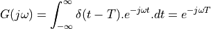
spectra of discrete-time signals. Consider the basic Dirac pulse  at time
  . The spectrum of this pulse is given by the Fourier Transform:
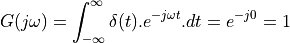
The spectrum of an impulse contains every frequency under the sun. Furthermore,
the magnitude and the phase of  have a particular format.
The amplitude of every phasor making up is
uniform, and they are all aligned with each other (at t=0). It is this alignment that causes such
a sharp impulse to appear in the time domain.
At any time besides t=0, the combination of frequencies in will cancel each other out,
so that the time-domain value of  .
.
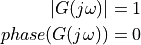
To see why, consider the behavior of the spectrum, as in the following picture.
Since  , each frequency contains a phasor of unit length. As time progresses, all of these phasors start to rotate at the speed corresponding to its frequency.
When
, each frequency contains a phasor of unit length. As time progresses, all of these phasors start to rotate at the speed corresponding to its frequency.
When  is positive, they rotate
counter-clockwise. When is negative, they rotate clockwise.
is positive, they rotate
counter-clockwise. When is negative, they rotate clockwise.
The reponse of the function in the time domain is the sum of all these phasors.
At time zero, all phasors (at every frequency) are aligned with the real axis, and
pointing upward. This makes  an infinitely high and infinitely narrow pulse with area 1.
If time advances one second, the phasors will rotate. After one second, the
phasor at
an infinitely high and infinitely narrow pulse with area 1.
If time advances one second, the phasors will rotate. After one second, the
phasor at  has made a half turn, while the phasor at
  has made a
full turn. The time domain response at time = 1 will be zero, since as the sum of all phasors (over all ) cancels out to 0. This is true for every
has made a
full turn. The time domain response at time = 1 will be zero, since as the sum of all phasors (over all ) cancels out to 0. This is true for every  , since it is always possible to find
a frequency
, since it is always possible to find
a frequency  that has made a full turn at that moment, thereby cancelling out
the response of frequencies between DC and .
that has made a full turn at that moment, thereby cancelling out
the response of frequencies between DC and .
The time-shifted Dirac Impulse
Next, consider the spectrum of a Dirac pulse at a time different from zero, say  for a
Dirac pulse at time
for a
Dirac pulse at time  . Clearly, this pulse must also contain the same frequency components as . The only difference is that has shifted over time , which will induce a delay for all of these frequency components. The spectrum is now given by:
The term  still has unit magnitude for all frequencies, but there is a phase shift
of
still has unit magnitude for all frequencies, but there is a phase shift
of  radians for the phasor at frequency .
The makes the term pretty important. This term describes the spectrum of a pulse delayed by time T. When we think of a sampled-data signal as a sequence of weighted pulses, we can thus construct the spectrum of the sampled-data signal by summing up the contribution of each pulse individually. Since the complete sampled data signal is a linear combination of weighted time-delayed pulses, the spectrum of a sampled data signal is a linear combination of the spectrum of these individual pulses.
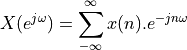
Indeed, let’s say that you have a sampled-data signal  .
Then the signal can be written in the time domain
as
.
Then the signal can be written in the time domain
as  as follows:

Now, making use of the linear property in frequency analysis, we can express the spectrum of as
the sum of the spectra caused by each single sample pulse. Mathematically:

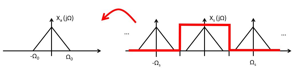
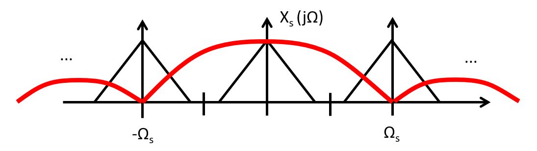
This is quite cool: you can describe the frequency spectrum of a sampled-data signal simply by looking at the sampled-data values! This transformation also demonstrates that the spectrum of a sampled-data signal is periodic,
since  is periodic. In particular, the period is
  . Indeed, recall from Lecture 1 that the spectrum of a sampled data signal contains infinitely many copies
of the spectrum of the baseband signal. When the baseband signal has no components below frequency
. Indeed, recall from Lecture 1 that the spectrum of a sampled data signal contains infinitely many copies
of the spectrum of the baseband signal. When the baseband signal has no components below frequency  , then the baseband signal can be perfectly recreated from the sampled-data signal.
The Discrete Time Fourier Transform
The previous expression is very close in form to the Discrete Time Fourier Transform.
Important
The Discrete Fourier Transform is the spectrum of a sample-data signal given a
normalized sample period of  .
.
Here are some well-known DTFT pairs.
Sequence |
Discrete-Time Fourier Transform |
|---|---|
|
1 |
|
|
1 |
|
|
|
|
|


The last formula, for  , is somewhat particular, since for many sample sequences it’s
not easy to find a closed form. That brings us to the z-Transform.
, is somewhat particular, since for many sample sequences it’s
not easy to find a closed form. That brings us to the z-Transform.
The z-Transform
The z-transform is a generalization of the DTFT where we write a sampled-data sequence as a power series
in  , where
 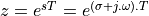 has both real and imaginary components.
The z-transform of a sampled-data signal becomes:

When equals the imaginary term  , then
 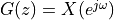 as in the DTFT.
However, in contrast to the DTFT, the z-transform is better at handling long series where summing
up
as in the DTFT.
However, in contrast to the DTFT, the z-transform is better at handling long series where summing
up 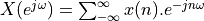 is complicated.
Here is an example. Suppose we have a unit step:

Which is tricky to sum up using  , since the sum does not converge for
  .
In the z-transform expression, we can rewrite
.
In the z-transform expression, we can rewrite  as a power series. Namely
Hence, the z-transform of the unit step can be written as
The choice of is inspired by the Laplace transform variable s. But unlike the Laplace transform,
the has built-in periodicity  .
.
The Unit Circle
z-transform functions are commonly represented (and computed) on a unit circle presentation,
which reflects the periodic nature of . In fact, the z-plane (which contains the
unit circle) is the discrete-time equivalent of the s-plane for continuous-time functions.
The inside of the unit circle corresponds to the left side of the s-plane (stable side) while
the outside of the unit circle corresponds to the right side of the s-plane. The unit circle
itself maps to the frequency axis in the s-plane, and any feature in the z-plane at an angle  will repeat forever in the s-plane at
 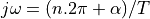 .
.
Signal Sampling on the MSP432
The MSP432 on the lab kit contains a 14-bit successive-approximation ADC.
The ADC is fully configurable from software. In the following, we summarize
the operation of the ADC as used by the XLAUDIO_LIB. Detailed
information on the MSP432 ADC can be found in the MSP432 Technical Reference
Manual.
First, let’s summarize the design abstraction levels that are relevant to understand the operation of sampling from a technical perspective. From the lowest abstraction level (i.e., closest to hardware) to the highest abstraction level (i.e., closest to the software application), we enumerate the abstraction levels as follows.
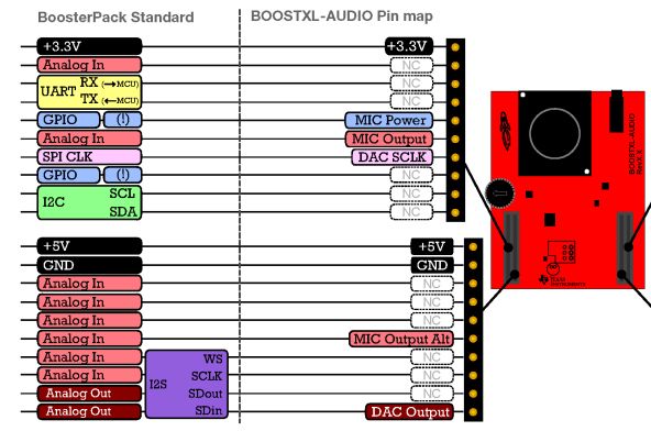
Hardware Schematics: The physical implementation of the MSPEXP432P401R board and the audio frontend BOOSTXL_AUDIO are each described in a user manual, the
MSPEXP432P401R User Guideand theAUDIO-BOOSTXL User Guide. These user guides show the physical connections of components on the board, including the connector pin definitions as well as the schematics.Hardware Details: Additional documentation on the hardware details of individual components on these PCB’s is captured in the datasheets for these components. For MSP432 is a fairly complex microcontroller, which has a
datasheetand a low-leveltechnical reference manual. The datasheet lists device-specific information (such as the precise configuration of pin-to-peripheral assignments), while the technical reference manual describes how to program the MSP432 peripherals.Hardware Abstraction Library: The low-level programming on the MSP432 is handled through a separate library (aptly named DriverLib) which is part of the MSP432P401R Software Development Kit. The documentation for this library can be found through CCS Resource Explorer. It can also be
downloaded as a PDFThis library introduces higher level functions that simplify peripheral programming.DSP Application Library: To make the programming of DSP applications on the MSP432 easier, we have added a software layer on top of the DriverLib. This software library, called XLAUDIO_LIB, was developed specifically for this class, and its documentation is available on the course website.
DSP Application: Finally, the application software forms the top of this stack. The application software for real-time DSP projects in this class will be written using a cyclic-executive model, ie. there is no RTOS involved.
Let’s consider these abstraction levels for the case of the loopback application of Lab 1.
Microphone Pre-amp
In the schematics of the AUDIO-BOOSTXL board, we find a schematic the microphone pre-amplifier:

This is a non-inverting op-amp configuration with a gain of approximately 250 (200000 / 820). At the output of the pre-amplifier, there’s a first-order low-pass filter with a cut-off frequency of 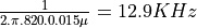 . Such lowpass filters are very common before analog-to-digital conversion, as they help ensure that the analog input signal is bandwidth limited.
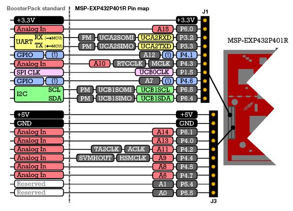
Next, the amplified microphone signal is wired to a header pin of the AUDIO-BOOSTXL board, and from there to a corresponding header pin on the MSP432 board. To find the pin definitions of each of these headers, you have to consult the User Guide for each board. The microphone is wired to the ‘Analog In’ pin of the BoosterPack header, which in turn is connect to a pin labeled A10 RTCLK MCLK P4.3. The important piece of information is A10, which stands for ‘ADC input channel 10’. That input pin is shared with several other microcontroller functionalities (RTCLK MCLK P4.3) - which will be inactive when we use the pin as an analog input pin.
MSP432 Microcontroller
We are now in the MSP432 microcontroller. The MSP432 datasheet gives a summary of the (large) amount of peripherals present in this microcontroller. One of them is the ADC. Signal samples are transported over the internal data bus to an ARM Cortex-M4F processor. The ARM Cortex-M4F is a RISC micro-processor with a three-stage pipeline.
The ‘F’ suffix in ‘Cortex-M4F’ indicates that the micro-processor has a built-in floating point unit. For our DSP experiments, this is an advantage as we can write C code using floating-point numbers. While floating-point accuracy is standard (and expected) on high-end processing platforms such as your laptop, is it considered a prime feature on micro-controllers. We will come back to this aspect in one of the future lectures.
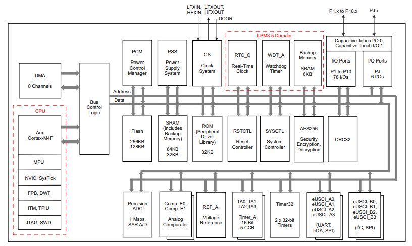
ADC14 Peripheral
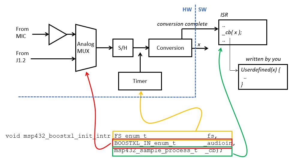
Next, we zoom in to the ‘Precision ADC’ block and consider the internal operation. The ADC has in input multiplexer that can select between one out of 23 analog sources. The ADC has a 14-bit resolution and uses a successive approximation architecture. The sample-and-hold operation which we discussed at the start of the lecture, is at the center of the ADC. The ADC conversion is started by asserting SAMPCON. It can be asserted by software (called a ‘software trigger’), are by an external source such as a timer. When the ADC conversion finishes, the module can optionally generate an interrupt.

In the Lab 1 loopback example, the ADC is used as follows. A timer module will trigger a conversion at regular intervals. With the XLAUDIO_LIB, the conversion rate can be selected between 8KHz and 48KHz. When the conversion in the ADC finishes, the ADC calls an end-of-conversion interrupt service routine (ISR). That ISR, in turn, can call a user-defined callback function. Your DSP code is integrated inside of this ISR callback function. Thus, with a conversion rate set at 16KHz, for example, your callback function is called 16,000 times per second, each time with a new converted output x.
The resolution of the ADC is 14 bit. With the input voltage 0V, the output code is 0x0000. With the input voltage 3V3, the output code is 0x3FFF (that is, 14 bits all set to ‘1’). In between, the encoded value increases linearly.
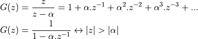
Signal Reconstruction
The conversion of a discrete sequence of numbers to a continuous-time signal
 is called signal reconstruction. Because of the Nyquist theorem, we know
that can be perfectly reconstructed by a simple filter operation.
is called signal reconstruction. Because of the Nyquist theorem, we know
that can be perfectly reconstructed by a simple filter operation.
Such a brick-wall filter is called an ideal reconstruction filter. It has an impulse response in the shape of a sinc function.
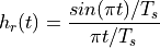
The sinc function interpolates between successive samples.  for every
value of
for every
value of  except for 0. The sinc function has a response for
  , which
means that it is non-causal and therefore cannot be implemented as is.
, which
means that it is non-causal and therefore cannot be implemented as is.
Here is the response of the filter on a single impulse in a stream of zero-valued samples.
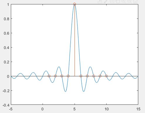
When the sample stream takes on random values, each of these random-valued pulses creates a sinc response, and all of these sinc combine to create an ideal (bandwidth-limited) interpolation of the sequence of random-valued pulses.
Practical Signal Reconstruction
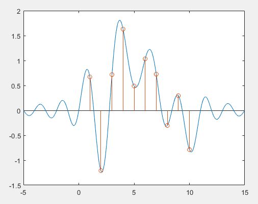
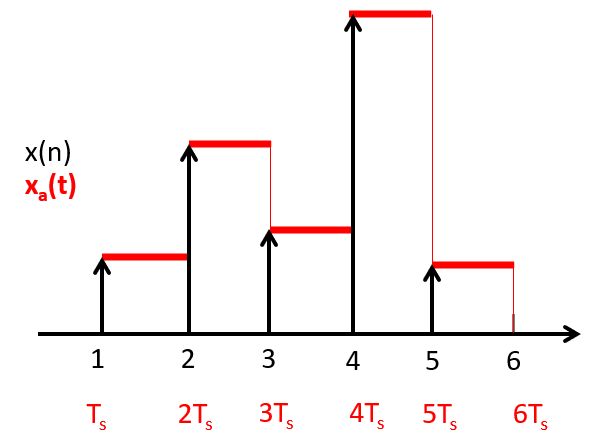
Because the ideal reconstruction filter cannot be implemented, in practice it is approximated. Many Digital-to-Analog converters, including the one used in our AUDIO-BOOSTXL kit, uses a zero-order hold reconstruction. The idea of a zero-order hold is to maintain the signal level of the previous pulse until the next pulse arrives. This leads to a staircase curve:
It’s useful to consider the distortion resulting from the zero-order hold reconstruction.
Clearly, the shape of the reconstructed is quite different from the one
which was originally sampled.
The zero-order hold reconstruction filter has an impulse reponse  :
:
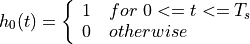
This reconstruction filter has the following frequency response:
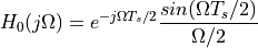
The important property of this frequency response is that it has zeroes at multiples
of the sample frequency,  . The effect of the zero-order hold filter on
the frequency response of the sampled-data signal
. The effect of the zero-order hold filter on
the frequency response of the sampled-data signal  shows the frequency
response of the imperfectly reconstructed .
shows the frequency
response of the imperfectly reconstructed .
Signal Reconstruction on the MSP432
The MSP432 does not have an on-board DAC. Instead, there is a 14-bit D/A converter on the AUDIO-XL board. This D/A converter is controller through an SPI interface on the MSP432, in addition to a SYNC pin.
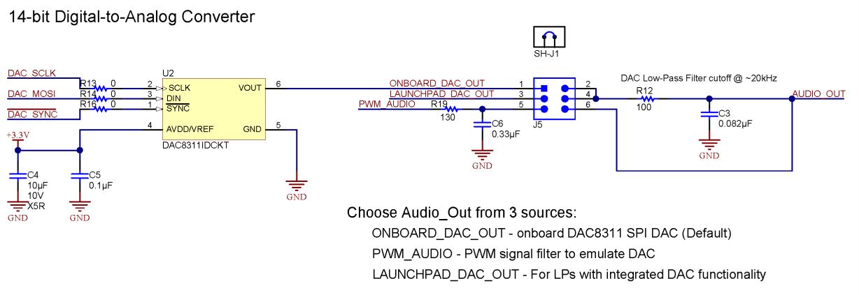
We first discuss the implementation on the AUDIOXL board, and next discuss the SPI
interface between the MSP432 and the AUDIO-XL board. The DAC is driven through a serial
SPI interface. The DAC has a zero-order hold response, and this response can be observed
by connecting an oscilloscope probe to pin 2 or pin 4 of connector J5. However, the signal
that is driving the audio amplifier is passed through a lowpass filter with a cutoff frequency
of approximately 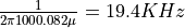 . This means that the sincx
effect of the staircase reconstruction may roll off quicker at higher frequencies. However,
when you generate signals with a sample frequency below 20KHz, you should be able to
observe parts of the sampled-data spectrum beyond the Nyquist frequency.
. This means that the sincx
effect of the staircase reconstruction may roll off quicker at higher frequencies. However,
when you generate signals with a sample frequency below 20KHz, you should be able to
observe parts of the sampled-data spectrum beyond the Nyquist frequency.
Note
In high-end audio systems, a signal construction filter would be much more sophisticated; it would eliminate any frequency beyond the Nyquist frequency, and it would eliminate the amplitude distortion caused by zero-order hold below the Nyquist frequency. The simplicity of the signal reconstruction hardware on our lab kit allows you to investigate the consequences of ‘imperfect’ signal reconstruction.
DAC8311 Chip
Next, we discuss the communication between the MSP432 and the DAC chip. The SPI interface communicates one byte at a time, so 14 bits for the DAC are transferred using a high byte and a low byte. The DAC has a SYNC pin which is asserted to indicate when the first byte is transmitted. The bits are transmitted MSB to LSB, and the DAC datasheet (DAC8311) illustrates the timing.
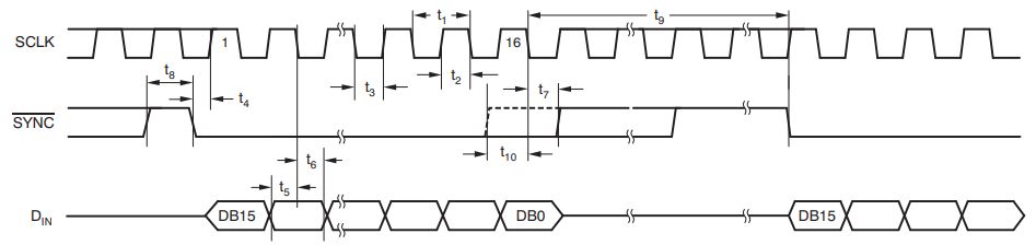
The MSP432_BOOSTXL library includes a software function, DAC8311_updateDacOut(uint16_t value),
which writes a new value to the DAC:
 1void DAC8311_updateDacOut(uint16_t value) {
 2    // Set DB15 and DB14 to be 0 for normal mode
 3    value &= ~(0xC000);
 4
 5    DAC8311_writeRegister(value);
 6}
 7
 8static void DAC8311_writeRegister(uint16_t data) {
 9    // Falling edge on SYNC to trigger DAC
10    GPIO_setOutputLowOnPin(DAC8311_SYNC_PORT,
11                           DAC8311_SYNC_PIN);
12
13    while (EUSCI_B_SPI_isBusy(DAC8311_EUSCI_BASE)) ;
14    EUSCI_B_SPI_transmitData(DAC8311_EUSCI_BASE, data >> 8); // high byte
15
16    while (EUSCI_B_SPI_isBusy(DAC8311_EUSCI_BASE)) ;
17    EUSCI_B_SPI_transmitData(DAC8311_EUSCI_BASE, data);  // low byte
18
19    while (EUSCI_B_SPI_isBusy(DAC8311_EUSCI_BASE)) ;
20
21    // Set SYNC back high
22    GPIO_setOutputHighOnPin(DAC8311_SYNC_PORT,
23                            DAC8311_SYNC_PIN);
24}
Distortion in the Sampling and Reconstruction Process
Finally, we summarize the sources of distortion in the sampling and reconstruction process. We can now understand the causes and effect of each type of distortion.
Aliasing is caused when a continuous-time signal is sampled at a rate below twice the highest frequency component in that continuous-time signal. Aliasing causes overlap between adjacent frequency bands in the discrete-time signal, and it causes non-recoverable distortion.
Quantization Noise is caused because the disrete-time signal is quantized on a finite number of quantization steps. Quantization noise is a non-linear effect, and its effect is often modeled as additive noise. We will investigate quantization noise in more detail when we discuss filters.
Jitter is caused by imperfect sampling, and is visible by random shifts back and forth in time. Jitter is a non-linear effect as well, and eventually appears as noise in the reconstructed signal.
Zero-order Hold is an effect in the signal reconstruction process where imperfect reconstruction is used instead of ideal sinc interpolation. A zero-order hold is a linear (filter) effect, which can be compensated by proper reconstruction filter design.