Saidoyoki: Evaluating side-channel leakage in pre- and post-silicon setting
Predicting the level and exploitability of side-channel leakage from complex SoC design is a challenging task. We present Saidoyoki, a test platform that enables the assessment of side-channel leakage under two different settings. The first is pre-silicon side-channel leakage estimation in SoC, and it requires the use of fast side-channel leakage estimation from a high-level design description. The second is post-silicon side-channel leakage measurement and analysis in SoC, and it requires a hardware prototype that reflects the design description. By designing an in-house SoC and next building a side-channel leakage analysis environment around it, we are able to evaluate design-time (pre-silicon) side-channel leakage estimates as well as prototype (post-silicon) side-channel leakage measurements. The Saidoyoki platform hosts two different SoC, one based on a 32-bit RISC-V processor and a second based on a SPARC V8 processor.
In our recent research, we have designed several ASICs as a byproduct (and often as a proof of concept) of our experimental work. FAMEv2 (Fault Aware Microprocessor Extensions) is an SoC with fault-sensing capability based around a LEON-3 core. PICO is a similar SoC based around a 32-bit RISC-V core. Both SoCs contain several coprocessors as well as on-chip RAM, and they are built in 180nm standard cells. Most importantly, they are in-house designs, so we have access to all design information down to layout level.
To study the problem of pre-silicon vs post-silicon side-channel leakage modeling, we integrated both of these SoCs in a test platform. The Saidoyoki board provides a programming interface to download applications to either chip, and supports high-bandwidth power measurement of each individual chip. The purpose of Saidoyoki is to validate a design flow for pre-silicon side-channel leakage estimation, by providing estimations next to actual side-channel leakage measurements. Our long term objectives are to understand and address two crucial shortcomings of side-channel leakage estimation from high-level models: (a) false positives, where the side-channel leakage estimation on the pre-silicon design model indicates side-channel leakage that cannot be confirmed by measurements; (b) false negatives, where the side-channel leakage estimation on the pre-silicon design does not show side-channel leakage while the measurements confirm the opposite. Both problems are hard and, to our knowledge, still unsolved.
The Saidoyoki Platform
This section describes the features of the Saidoyoki platform, including the platform architecture, and the system architecture of the chips.
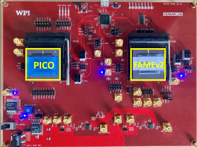
Saidoyoki PCB
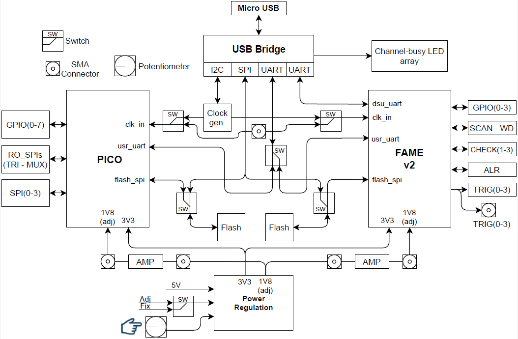
A side-channel measurement setup includes a test target, a means to digitize power side-channel leakage, and a side-channel campaign controller. The controller exchanges stimuli with the test target, and while the target executes the stimuli, the target’s power signature is captured. Afterwards, the campaign controller collects the power signatures and performs side-channel analysis. A PCB to support a test target thus has to provide multiple functions, including (a) providing easy access to the power consumption of the target, (b) real-time data input/output to exchange test stimuli with the campaign controller, (c) debugging of programmable/reconfigurable targets, and optionally, (d) adjusting target voltage/clock to study the impact of environmental factors. The Saidoyoki PCB was developed to support the PICO and FAME chips as targets for side-channel measurement campaigns, and it supports all functions enumerated above.
The board is connected to the side-channel campaign controller with a single USB connection to multiplex multiple data and control channels used in a campaign (FT4232HL USB Bridge IC). These control channels include a UART debug connection for FAMEv2, a shared user UART, a shared SPI to program flash memories, and an I2C control channel for clock configuration.
The side-channel leakage of each ASIC is captured by measuring voltage drop over a shunt resistor. The signal is also amplified through a differential broadband opamp, one for each ASIC. Saidoyoki uses a single 5V power supply that is regulated into a fixed 3V3 supply and an adjustable 1V8 supply. The adjustable supply feeds the ASIC core and can be varied between 1V and 2V. This rail is also split into two using ferrite beads and then connected to each chip independently. A precise shunt resistor is inserted into each branch of the 1.8V rail for power measurement.
The flash chips connected to PICO and FAMEv2 are externally programmable through USB. The board has several 3-point slider switches to physically switch the flash chips from external configuration to ASIC configuration. In the ASIC configuration, the ASIC will boot from the firmware configured in the flash chips.
Saidoyoki also includes a clock generation IC (SI5351A-B-GTR), which is able to generate configurable clock frequencies for the ASICs between 2.5KHz and 200MHz. The clock can also be provided from an external source through an SMA connector.
Finally, the Saidoyoki board supports low-level debugging tasks by bringing every chip pin out on a jumper header or an SMA connector. Additionally, the GPIO ports in each ASIC are visible through LEDs.
FAME2 ASIC
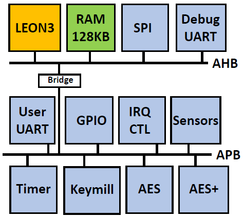
The FAMEv2 ASIC is a 180nm SoC with a LEON3 core and 128 kByte of internal memory, and several coprocessors. The program can execute either from on-chip SRAM or else from off-chip flash through an SPI flash ROM. A debug unit, controlled through an on-chip Debug UART, provides program loading, monitoring, breakpoints. The coprocessors are isolated from the processor through a bus bridge. All coprocessors exclusively operate as bus slaves, and communicate with the software through memory-mapped registers. FAME contains cryptographic accelerators for symmetric-key encryption (AES and AES+, a hardened version of AES) and pseudo-random stream generation (KeyMill). The sensors in FAME detect timing faults injected through clock glitching and voltage glitching.
PICO ASIC
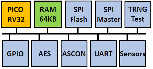
The PICO ASIC is a 180nm SoC with a RISCV (RV32) core and 64 kByte of internal memory, and several coprocessors. The program exclusively runs from off-chip flash through a Quad-SPI flash ROM. The system is integrated on a single bus. All coprocessors run as bus slaves and communicate with the RISC-V software through memory-mapped registers. PICO contains cryptographic accelerators for symmetric-key encryption (AES), authenticated encryption (ASCON), and hardware testing of true random bitstreams (TRNG test). The sensors in PICO detect fault injection as well as side-channel leakage.
Pre-silicon Side-channel Leakage Estimation
![]()
In a pre-silicon setting, power-based side-channel leakage is estimated through a time-based simulation of the power consumption of the target.
The Saidoyoki flow starts from a gate-level netlist, obtained from the FAME/PICO chip design or else through RTL synthesis of the design flows. Through a suitable testing scenario, a set of testing stimuli are defined. For classic DPA/CPA analysis of cryptographic hardware, for example, one selects a fixed key and a set of random plaintext/ciphertext. Specific or non-specific TVLA tests, on the other hand, require a combination of random and fixed key/plaintext inputs. The activity files created from hardware simulation are used by a time-based power simulation tool, which provides a trace for every input test vector. Finally, the stimuli, activity files and traces are used as input for the side-channel evaluation. Our prototype implementation supports Cadence Genus or Synopsys Design Compiler, Cadence XCelium or Mentor ModelSim, and Cadence Joules respectively as synthesis, simulation, and power estimation tool. The side-channel evaluation is a customized Chipwhisperer script.
There is a trade-off between the level of simulation detail, and the ability of a design model to capture different causes and sources of side channel leakage. The gate-level abstraction provides reasonable accuracy. Because of the post-silicon artifacts available in Saidoyoki, we prefer lower simulation abstraction levels to investigate and verify lower-level effects.
To ensure sufficient accuracy with software and SoC firmware targets, we extend the hardware based flow and simulate the microprocessor as a gate-level design as well. The main challenge is to convert the firmware into a form that can be integrated into the SoC hardware simulation. We compile the firmware into a binary that is used to initialize the on-chip memory at the start of the simulation. By compiling input test vectors (key, input) as hard-coded constants in the firmware binary, we also eliminate complex input/output schemes during simulation.
To enable testing only specific parts of the firmware, we make use of the GPIOs on the SoC as triggers. We set a GPIO pin high right before the point of interest and reset it to low right after. In the test bench module, during simulation, we monitor the trigger signal and log its set and reset time stamps. Later, in power trace generation phase, we generate the power trace only for the logged time period.
Post-silicon Side-channel Leakage Estimation
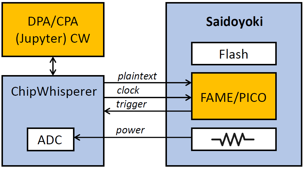
Measuring side-channel leakage in the post-silicon setting requires a campaign controller to measure power from the PICO or FAME chips on Saidoyoki while they execute a test application. We use a Chipwhisperer kit. Chipwhisperer uses synchronous sampling and generates a clock signal for the target. This allows the side-channel leakage to be captured with low overhead of one to four times the target clock. A campaign executes a large collection of encryption operations on the target, with different input stimuli. For each operation, Chipwhisperer sends an input plaintext. The target responds with a trigger when the cryptographic operation starts. Chipwhisperer then collects the power signal and finally performs side-channel leakage analysis or assessment.
Further Reading
| P. Schaumont, "You Can Hide But You Can't Verify: On Side-channel Countermeasure Verification," Workshop on SSH-SoC: Safety and Security in Heterogeneous Open System-on-Chip Platforms, July 2023. | |
| preprint doi | P. Kiaei, Z. Liu, P. Schaumont, "Leverage the Average: Averaged Sampling in Pre-Silicon Side-Channel Leakage Assessment," Great Lakes Symposium on VLSI, June 2022. |
| preprint | P. Kiaei, Z. Liu, R. K. Eren, Y. Yao, P. Schaumont, "Saidoyoki: Evaluating Side-channel Leakage in Pre- and Post-silicon Setting," IEEE SOCC 2021, September 2021. Preprint IACR ePrint Archive: Report 2021/1235. |
| Y. Yao, P. Kiaei. R. Singh, S. Tajik, P. Schaumont, "Programmable RO (PRO): A Multipurpose Countermeasure against Side-channel and Fault Injection Attack," arXiv:2106.13784, 2021. | |
| doi | Y. Yao, P. Schaumont, J. van Woudenberg, C.B. Breunesse, E. M. Santillan, S. Stecyk, "Verification of Power-based Side-channel Leakage through Simulation," 63rd IEEE International Midwest Symposium on Circuits and Systems, August 2020. |
| doi | B. Yuce, C. Deshpande, M. Ghodrati, A. Bendre, L. Nazhandali, P. Schaumont, "A Secure Exception Mode for Fault-Attack-Resistant Processing" IEEE Transactions on Dependable and Secure Computing, 16(3):388-401, 2019. |