Attention
This document was last updated Aug 22 24 at 21:58
Optimized 32-bit CORDIC Module for GPDK45
Important
The purpose of this lab is as follows.
Study a high-level reference implementation of the CORDIC algorithm in C, including a reference testbench with 1024 test vectors.
Select an optimization strategy (Area or Throughput) and develop an RTL implementation of the CORDIC algorithm, and verify the correctness of the design using the same set of test vectors. Optimizing for area means that your final design must be as small as possible in terms of layout area. Optimizing for throughput means that your final design must compute as many test vectors per second as possible at the maximum clock speed possible with the implemented layout.
Synthesize the design into GPDK45 standard cells. Perform static timing analysis on the design result and demonstrate that your design meets timing.
Create a layout for the design. Perform parastic extraction. Perform static timing analysis on the post-route design and demonstrate that your design meets timing. Perform gate-level simulation using back-annotated post-route timing and demonstrate that your design simulation correctly computes the set of 1024 test vectors.
Summarize your design result in a written report.
Attention
The due date of this lab is 10 November
Introduction
The CORDIC algorithm is an algorithm that efficiently computes transcendental functions (sine, cosine, tangent). CORDIC stands for COordinate Rotation DIgital Computer. The remarkable property of CORDIC is that it requires only integer arithmetic and yet can obtain highly accurate approximutions of sine and cosine functions. There is extensive online documentation of this algorithm, so this lab assigment does not elaborate furter on the algorithm. Some examples references are the following.
Meher, J. Valls, T. -B. Juang, K. Sridharan and K. Maharatna, “50 Years of CORDIC: Algorithms, Architectures, and Applications,” in IEEE Transactions on Circuits and Systems I: Regular Papers, vol. 56, no. 9, pp. 1893-1907, Sept. 2009, doi: 10.1109/TCSI.2009.2025803.
Schaumont, P.R. (2010). CORDIC Coprocessor. In: A Practical Introduction to Hardware/Software Codesign. Springer, Boston, MA. doi:10.1007/978-1-4419-6000-9_12
The purpose of this lab is to build an optimized hardware implementation of this algorithm in GPDK45 standard cells. You will go through all steps of Digital Design that we discussed so far: RTL design and optimization, RTL synthesis, static timing analysis, layout, gate-level simulation and gate-level static timing analysis.
Important
In the context of this lab, optimzation means that your design is the best among all submissions. You can optimized for area (layout area as small as possible) or for throughput (final design as fast as possible), so there will be two ‘best’ designs. A portion of your lab grade is directly derived from the rank of your design in the overall ranking in terms of the selected optimization criteria.
You need/may submit only one design, and you may select only one optimization criteria.
Reference Implementation
After you have accepted the assignment, a starter repository will be available for you. Clone it to the design server (your repo name includes your account name).
git clone git@github.com:wpi-ece574-f23/lab-2-patrickschaumont.git
You will obtain the following lab directory structure:
refC |
Reference Implementation in C. Golden model and testvectors |
refV |
Behavioral Implementation in Verilog. Defines the testbench |
rtl |
A Sample RTL implementation of a multiplexed solution |
constraints |
Constraints for the sample RTL implementation |
sim |
Simulation for the sample RTL implementation |
syn |
RTL synthesis for the sample RTL implementation |
sta |
Static timing analysis for the sample RTL implementation |
layout |
Layout for the sample RTL implementation |
glsim |
Gate level simulation for the sample RTL implementation |
glsta |
Gate level STA for the sample RTL implementation |
The golden model is in refC. It contains a CORDIC implementation that computes
sine/cosine of angles in the first quadrant, with a precision of 32 bits and 28
fractional bits (FIX<32,28>). You can compile and run this reference implementation:
cd refC
make
./cordic
Running this program will produce a set of test vectors:
rad  c12ac7f cos  ba83bca sin  af5a193 rad +0.7546 cos +0.7286 sin +0.6850 verif cos +0.7286 sin +0.6850
rad  31102e9 cos  fb5011c sin  30c37cf rad +0.1917 cos +0.9817 sin +0.1905 verif cos +0.9817 sin +0.1905
rad  bfb8eb2 cos  bb80511 sin  ae4bea8 rad +0.7489 cos +0.7324 sin +0.6808 verif cos +0.7324 sin +0.6808
In this table, rad represents an encoded input in radians, and cos and sin represent an encoded output. The hex numbers in this output represent FIX<32,28> fixed point numbers. For example, c12ac7f represent a fractional number in radians equal to c12ac7f/(1 << 28) = 0.7546.
This pattern rad, cos, sin is repeated three times. The first is the input/output of the C program in FIX<32,28>. The second group is the input/output of the C program as floating point numbers. The third group is the verification computed using functions of the C math library.
Running this program also creates a test vector file, vectors.txt. The test vector file has three columns: the 32-bit input, and two 32-bit outputs. The output columns can be used to verify the Verilog implementation.
Important
Your design is correct only if it simulates every test vector in vectors.txt correctly. Before proceeding to synthesis/layout, make sure that your RTL design is correct.
Verilog Reference Module
Your design must provide the following I/O ports.
module cordic(
              input wire                clk,
              input wire                reset,
              input wire                start,
              input wire signed [31:0]  target,
              output wire signed [31:0] X,
              output wire signed [31:0] Y,
              output wire               done
              );
clk |
I |
positive-edge-triggered clock |
reset |
I |
synchronous active-high reset |
start |
I |
synchronous active-high load signal |
target |
I |
32-bit target input, read when start=1 |
X, Y |
O |
32-bit output with sine and cosine components |
done |
O |
active-high completion signal, mark XY valid |
Verilog Testbench Implementation
The refV directory contains a behavioral (non-synthesizable) Verilog implementation
of the CORDIC module, along with a testbench cordictb.v. This testbench
drives the input/output ports of the CORDIC module with the testvectors
generated under refC. You can reuse this testbench for later testing of the RTL
and gate-level design of your CORDIC.
To simulate, run the testbench as follows.
cd refV
make
You will see the output for each testvector followed by the message ‘TESTBENCH PASSES’. If you don’t see that message, your design is not correct and you have to debug the RTL before continuing.
target 0c12ac7f X 0ba83bca chkX 0ba83bca Y 0af5a193 chkY 0af5a193 OK 1
target 031102e9 X 0fb5011c chkX 0fb5011c Y 030c37cf chkY 030c37cf OK 1
target 0bfb8eb2 X 0bb80511 chkX 0bb80511 Y 0ae4bea8 chkY 0ae4bea8 OK 1
target 00a06e71 X 0ffcdbd8 chkX 0ffcdbd8 Y 00a0625b chkY 00a0625b OK 1
target 1074b5bf X 0841fae1 chkX 0841fae1 Y 0db451be chkY 0db451be OK 1
target 0b414d96 X 0c33af6b chkX 0c33af6b Y 0a597de0 chkY 0a597de0 OK 1
TESTBENCH PASSES
Sample RTL Implementation
To illustrate what steps you have to take during your design, you get one sample solution of an RTL implementation. This design is a multiplexed solution that has not been particularly optimized for area nor throughput. While you may start for your final solution from this design, it’s likely that you may not end up with a good performance rank (since everybody has access to this solution).
To simulate the sample solution:
cd sim
make
To perform RTL synthesis, see below. Note that this is where you select the clock period of your design. The sample RTL implementation is implemented at a clock period of 8ns. Also, note that the RTL synthesis makes use of the constraints SDC file in constraints.
cd syn
make
You can verify that this design meets timing:
cat reports/cordic_report_qor.rpt

Timing
--------

Clock Period
-------------
clk   8000.0


  Cost    Critical         Violating
 Group   Path Slack  TNS     Paths
-------------------------------------
clk          1437.1   0.0          0
default    No paths   0.0
-------------------------------------
Total                 0.0          0

Instance Count
--------------
Leaf Instance Count             1261
Physical Instance count            0
Sequential Instance Count        136
Combinational Instance Count    1125
Hierarchical Instance Count        0

Area
----
Cell Area                          2918.628
Physical Cell Area                 0.000
Total Cell Area (Cell+Physical)    2918.628
Net Area                           0.000
Total Area (Cell+Physical+Net)     2918.628
After synthesis, you also perform static timing analysis:
cd sta
make
In particular, refer to the first path in late.rpt to check the critical path of your design.
cat late.rpt

Path 1: MET Setup Check with Pin Yr_reg[31]/CK
Endpoint:   Yr_reg[31]/D (^) checked with  leading edge of 'clk'
Beginpoint: A_reg[5]/Q   (^) triggered by  leading edge of 'clk'
Path Groups: {clk}
Other End Arrival Time          0.000
- Setup                         0.119
+ Phase Shift                   8.000
= Required Time                 7.881
- Arrival Time                  6.484
= Slack Time                    1.397
     Clock Rise Edge                 0.000
     + Clock Network Latency (Ideal) 0.000
     = Beginpoint Arrival Time       0.000
      -----------------------------------------------------------------------------------
      Instance                           Arc           Cell      Delay  Arrival  Required
                                                                        Time     Time
      -----------------------------------------------------------------------------------
      A_reg[5]                           CK ^          -         -      0.000    1.397
      A_reg[5]                           CK ^ -> Q ^   DFFHQX1   0.186  0.186    1.583
      gt_88_21_g2159__5477               AN ^ -> Y ^   NAND2BX1  0.082  0.268    1.665
      gt_88_21_g2109__2802               A2 ^ -> Y v   AOI32X1   0.155  0.423    1.820
      gt_88_21_g2098__6417               A1 v -> Y ^   OAI211X1  0.150  0.573    1.970
      gt_88_21_g2087__1881               A0 ^ -> Y v   OAI211X1  0.167  0.740    2.137
      g6174                              A1 v -> Y v   AO21XL    0.145  0.885    2.282
      gt_88_21_g2084__8246               B v -> Y ^    NAND2X1   0.033  0.918    2.315
      gt_88_21_g2083__5122               A1 ^ -> Y v   AOI21X1   0.102  1.020    2.417
      g6168                              A v -> Y ^    INVX2     0.164  1.184    2.581
      add_90_38_Y_sub_90_49_g2874        A ^ -> Y v    INVX2     0.197  1.381    2.778
      add_90_38_Y_sub_90_49_g2873__4733  A v -> Y ^    MXI2XL    0.167  1.548    2.945
      add_90_38_Y_sub_90_49_g2792__5477  CI ^ -> CO ^  ADDFX1    0.217  1.765    3.162
      add_90_38_Y_sub_90_49_g2791__6417  CI ^ -> CO ^  ADDFX1    0.186  1.951    3.348
      add_90_38_Y_sub_90_49_g2790__7410  CI ^ -> CO ^  ADDFX1    0.186  2.137    3.534
      add_90_38_Y_sub_90_49_g2789__1666  CI ^ -> CO ^  ADDFX1    0.186  2.323    3.720
      add_90_38_Y_sub_90_49_g2788__2346  CI ^ -> CO ^  ADDFX1    0.186  2.509    3.906
      add_90_38_Y_sub_90_49_g2787__2883  CI ^ -> CO ^  ADDFX1    0.186  2.695    4.092
      add_90_38_Y_sub_90_49_g2786__9945  CI ^ -> CO ^  ADDFX1    0.186  2.881    4.278
      add_90_38_Y_sub_90_49_g2785__9315  CI ^ -> CO ^  ADDFX1    0.188  3.069    4.466
      add_90_38_Y_sub_90_49_g2784__6161  C ^ -> Y v    NAND3BXL  0.108  3.177    4.574
      add_90_38_Y_sub_90_49_g2783__4733  C0 v -> Y ^   OAI211X1  0.093  3.270    4.667
      add_90_38_Y_sub_90_49_g2779__6131  CI ^ -> CO ^  ADDFX1    0.212  3.482    4.879
      add_90_38_Y_sub_90_49_g2778__7098  CI ^ -> CO ^  ADDFX1    0.186  3.668    5.065
      add_90_38_Y_sub_90_49_g2777__8246  CI ^ -> CO ^  ADDFX1    0.186  3.854    5.251
      add_90_38_Y_sub_90_49_g2776__5122  CI ^ -> CO ^  ADDFX1    0.186  4.040    5.437
      add_90_38_Y_sub_90_49_g2775__1705  CI ^ -> CO ^  ADDFX1    0.186  4.226    5.623
      add_90_38_Y_sub_90_49_g2774__2802  CI ^ -> CO ^  ADDFX1    0.188  4.414    5.811
      add_90_38_Y_sub_90_49_g2773__1617  C ^ -> Y v    NAND3BXL  0.134  4.548    5.945
      add_90_38_Y_sub_90_49_g2769__8428  A1 v -> Y ^   OAI221X1  0.172  4.720    6.117
      add_90_38_Y_sub_90_49_g2763__6417  A2 ^ -> Y v   AOI31X1   0.171  4.891    6.288
      add_90_38_Y_sub_90_49_g2758__9945  A1 v -> Y ^   OAI21X1   0.110  5.001    6.398
      add_90_38_Y_sub_90_49_g2755__4733  A1 ^ -> Y v   AOI21X1   0.116  5.117    6.514
      add_90_38_Y_sub_90_49_g2753__5115  C v -> Y v    OR3XL     0.171  5.288    6.685
      add_90_38_Y_sub_90_49_g2749__8246  A1 v -> Y ^   OAI221X1  0.093  5.381    6.778
      add_90_38_Y_sub_90_49_g2746__2802  CI ^ -> CO ^  ADDFX1    0.219  5.600    6.997
      add_90_38_Y_sub_90_49_g2745__1617  CI ^ -> CO ^  ADDFX1    0.186  5.786    7.183
      add_90_38_Y_sub_90_49_g2744__3680  CI ^ -> CO ^  ADDFX1    0.186  5.972    7.369
      add_90_38_Y_sub_90_49_g2743__6783  CI ^ -> CO ^  ADDFX1    0.184  6.156    7.553
      add_90_38_Y_sub_90_49_g2742__5526  B ^ -> Y ^    XNOR2X1   0.163  6.319    7.716
      g6091__4733                        A1 ^ -> Y ^   AO22XL    0.165  6.484    7.881
      Yr_reg[31]                         D ^           DFFHQX1   0.000  6.484    7.881
      -----------------------------------------------------------------------------------
The next step is to generate the layout. Note that the layout makes use of
the chip I/O pin constraints in chip/chip.io. The synthesis step of the layout directly
reads the synthesis netlist produced in syn. Hence, you must complete RTL synthesis
before building the layout.
cd layout
make syn
make layout
When the layout run ends, the script prints the final core area. This is the number that will be used for area cost of your design. This design would measure 6140.61 square micron.
FINAL DESIGN CORE AREA:
@file 173: puts [expr ($xu - $xl)*($yu - $yl)]
6140.61
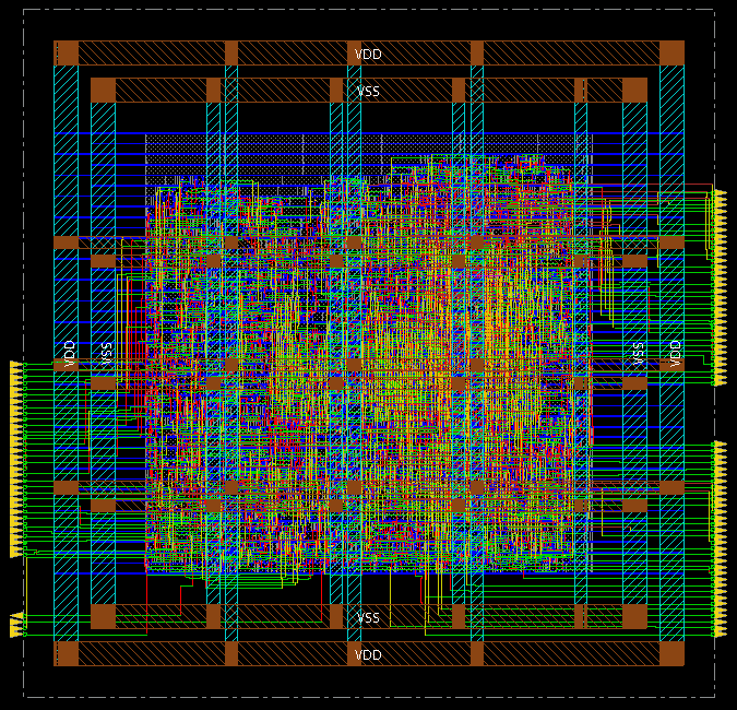
You can inpect the layout with the gui_show command.
Pay particular attention to white crosses in your design, which indicate design violation errors.
While we did not discuss design violations in detail, a correct design should avoid them. Design
violations can occur because of overly tight design constraints.
After layout, you can run gate-level simulation
cd glsim
make
The testbench must of course still pass
...
target 00a06e71 X 0ffcdbd8 chkX 0ffcdbd8 Y 00a0625b chkY 00a0625b OK 1
target 1074b5bf X 0841fae1 chkX 0841fae1 Y 0db451be chkY 0db451be OK 1
target 0b414d96 X 0c33af6b chkX 0c33af6b Y 0a597de0 chkY 0a597de0 OK 1
TESTBENCH PASSES
Finally, you can run gate-level static timing analysis.
cd glsta
make
The design must still meet timing, i.e. have a positive slack.
Path 1: MET Setup Check with Pin Xr_reg[31]/CK
Endpoint:   Xr_reg[31]/D (^) checked with  leading edge of 'clk'
Beginpoint: T_reg[2]/Q   (v) triggered by  leading edge of 'clk'
Path Groups: {clk}
Other End Arrival Time          0.104
- Setup                         0.113
+ Phase Shift                   8.000
= Required Time                 7.991
- Arrival Time                  7.641
= Slack Time                    0.350
     Clock Rise Edge                 0.000
     + Clock Network Latency (Prop)  0.104
     = Beginpoint Arrival Time       0.104
      ----------------------------------------------------------------
      Instance       Arc           Cell       Delay  Arrival  Required
                                                     Time     Time
      ----------------------------------------------------------------
      T_reg[2]       CK ^          -          -      0.104    0.454
      T_reg[2]       CK ^ -> Q v   DFFHQX1    0.262  0.366    0.716
      g37105         A v -> Y ^    NAND2X1    0.060  0.426    0.776
      g36792         C ^ -> Y v    NAND3BXL   0.143  0.568    0.919
      g36636         A v -> Y ^    NAND3X1    0.136  0.705    1.055
      g37800         B0 ^ -> Y v   OAI21X1    0.098  0.803    1.153
      g36385__2802   B0 v -> Y ^   OAI21X1    0.065  0.868    1.218
      g36369__2883   B0 ^ -> Y v   AOI2BB1X1  0.073  0.942    1.292
      g36293__4319   A2 v -> Y ^   OAI31X1    0.143  1.084    1.434
      g36290__2398   A2 ^ -> Y v   AOI31X1    0.245  1.329    1.680
      g36289__5477   A v -> Y ^    NAND3X1    0.148  1.477    1.827
      g36288__6417   A ^ -> Y v    NAND2X1    0.123  1.601    1.951
      FE_OFC7_n_938  A v -> Y v    CLKBUFX6   0.203  1.804    2.154
      g36287         A v -> Y ^    CLKINVX6   0.153  1.957    2.307
      g36196__2883   B ^ -> Y ^    MX2X1      0.254  2.211    2.561
      g36013__5477   B0 ^ -> Y v   AOI2BB1X1  0.075  2.286    2.636
      g35937__6131   B v -> Y ^    NOR2X1     0.082  2.368    2.719
      g35874__1705   A1 ^ -> Y v   OAI21X1    0.131  2.500    2.850
      g35847__6131   A1 v -> Y ^   AOI21X1    0.130  2.630    2.980
      g35816__5115   B0 ^ -> Y v   AOI2BB1X1  0.085  2.715    3.065
      g35809__2802   B v -> Y ^    NOR2X1     0.089  2.803    3.153
      g35792__2883   B0 ^ -> Y v   AOI2BB1X1  0.087  2.890    3.240
      g35790__9315   B v -> Y ^    NOR2X1     0.084  2.974    3.325
      g35758__2883   A1 ^ -> Y v   OAI21X1    0.130  3.105    3.455
      g35730__5477   A1 v -> Y ^   AOI22X1    0.158  3.263    3.613
      g35704__6783   A1 ^ -> Y v   OAI21X1    0.165  3.428    3.778
      g35674__1705   A1 v -> Y ^   AOI21X1    0.140  3.567    3.917
      g35655__2883   A1 ^ -> Y v   OAI21X1    0.163  3.730    4.080
      g37644         B0 v -> Y v   OA21X1     0.149  3.879    4.229
      g35620__5107   B v -> Y ^    NOR2X1     0.074  3.953    4.303
      g35597__5122   B0 ^ -> Y v   AOI2BB1X1  0.083  4.037    4.387
      g35595__2802   B v -> Y ^    NOR2X1     0.083  4.120    4.470
      g35573__4733   A1 ^ -> Y v   OAI21X1    0.150  4.270    4.620
      g35548__6417   B1 v -> Y ^   AOI22X1    0.161  4.431    4.781
      g35520__8428   B0 ^ -> Y v   AOI2BB1X1  0.110  4.541    4.891
      g35518__6260   B v -> Y ^    NOR2X1     0.105  4.645    4.996
      g35488__6783   A1 ^ -> Y v   OAI21X1    0.157  4.803    5.153
      g35466__1881   B v -> Y ^    NAND2X1    0.102  4.905    5.255
      g35454__4319   B ^ -> Y v    NOR2X1     0.069  4.974    5.324
      g35428__3680   B1 v -> Y ^   AOI221X1   0.175  5.148    5.499
      g35401__5115   A1 ^ -> Y v   OAI21X1    0.204  5.352    5.702
      g35378         A v -> Y ^    INVX1      0.108  5.461    5.811
      g35365__9315   A1 ^ -> Y v   OAI21X1    0.123  5.584    5.934
      g35350         A v -> Y ^    INVX1      0.102  5.685    6.036
      g35339__4319   A1 ^ -> Y v   OAI21X1    0.098  5.784    6.134
      g35336         A v -> Y ^    INVX1      0.075  5.859    6.209
      g35323__6161   A1 ^ -> Y v   OAI21X1    0.113  5.972    6.323
      g35299__5107   B v -> Y ^    NAND2X1    0.108  6.080    6.430
      g35287__6161   A1 ^ -> Y v   OAI21X1    0.124  6.204    6.554
      g35281         A v -> Y ^    INVX1      0.093  6.297    6.647
      g35253__9315   A1 ^ -> Y v   OAI21X1    0.109  6.406    6.756
      g35238__1617   A1 v -> Y ^   AOI22X1    0.158  6.564    6.914
      g35214__6161   A1 ^ -> Y v   OAI22X1    0.188  6.752    7.102
      g37699         CI v -> CO v  ADDFX1     0.245  6.996    7.346
      g35194         A v -> Y ^    INVX1      0.072  7.068    7.418
      g35184__2883   A1 ^ -> Y v   OAI22X2    0.141  7.210    7.560
      g35170__5122   B v -> Y v    XNOR2X1    0.181  7.391    7.741
      g35163__6783   A1 v -> Y ^   AOI21X1    0.078  7.469    7.819
      g35160__8428   B0 ^ -> Y v   OAI21X1    0.103  7.573    7.923
      g35158__4319   B0 v -> Y ^   OAI2BB1X1  0.069  7.641    7.991
      Xr_reg[31]     D ^           DFFX2      0.000  7.641    7.991
Performance Metrics
The performance metrics used in this lab differ slightly from the convention we have adopted in Lecture 8.
When you optimize for area, the final area of your design is the core area as reported by the
run_innovus.tclscript.When you optimize for throughput, your final throughput is the maximum clock frequency achieved by your design times the number of clock cycles per output. For example, the sample RTL implementation has a cycle budget of 22 cycles and a maximum clock frequency of 125MHz, so the throughput of this design is 5.682 million CORDIC evaluations per second.
The differences of these metrics with our earlier convention is as follows: To define area, we use physical core area, while previously we have used the active area (the area of the standard cells). To define throughput, we determine the clock frequency through the clock period constraint you use for your design, and not the critical path.
Grading Rubric
The lab receives 100 points, to be distributed as follows.
20 points for the RTL design: correctness and quality of the code and the testbench
20 points for the synthesis result: design synthesizes correctly (no latches), meets advertised timing, meets input/output specification
20 points for the layout: design has a layout that meets timing, that has no design violations
20 points for the rank of your design within the category you choose to optimize for (area/throughput). The rank-1 design gets 20 points, the rank-2 design gets 18 points, and so on.
20 points for your report: clearly document your design process, include listings, include tables with area and critical path, include a snapshot of the layout.
Attention
The following are important report requirements.
Use a typesetting tool such as latex or word. Do not submit handwritten scanned reports.
Use a screen capture tool to collect graphics such as layout information. Do not use your smartphone to take a picture from the screen.
Be clear and complete in your report. I am not looking for the correct solution; I am looking to understand your solution. Explain the steps that lead up to a result. The report does not have a minimum length nor a maximum length, as long as it is clear what you did and your answers to questions are complete.
Make sure to update, commit and push the results of your lab to your repository. You do not have to turn in anything on Canvas. All results will be communicated through your github repository.