Attention
This document was last updated Aug 22 24 at 21:58
Arithmetic
Important
The purpose of this lecture is as follows.
To discuss the efficient implementation of several arithmetic operations
To define the role of scheduling in designing multi-cycle operations
To define bit-serial arithmetic structures
To describe fast adder implementations based on prefix carry chain
Attention
The following are publications that are relevant to this lecture.
JP Deschamps, GD Sutter, E Canto, “Guide to FPGA Implementation of Arithmetic Functions,” Springer 2012. A good reference on the design and implementation of Arithmetic in Hardware. https://link.springer.com/book/10.1007/978-94-007-2987-2.
Brent and Kung, “A Regular Layout for Parallel Adders,” in IEEE Transactions on Computers, vol. C-31, no. 3, pp. 260-264, March 1982, doi: 10.1109/TC.1982.1675982. https://ieeexplore.ieee.org/document/1675982
Harris, “A taxonomy of parallel prefix networks,” The Thrity-Seventh Asilomar Conference on Signals, Systems & Computers, 2003, 2003, pp. 2213-2217 Vol.2, doi: 10.1109/ACSSC.2003.1292373. https://ieeexplore.ieee.org/abstract/document/1292373/
Hartley, K. Parhi, “Digit-serial Computation,” Springer 1995. A good reference on bit-serial design. https://link.springer.com/book/10.1007/978-1-4615-2327-7
Parhami, “Computer Arithmetic,” Oxford University Press 2009. https://web.ece.ucsb.edu/~parhami/text_comp_arit.htm. Standard text on computer arithmetic.
Introduction
Number crunching is the single most important task done by Digital Hardware. Algorithms transform numbers and symbols into results using operations that, eventually, always rely on arithmetic. Arithmetic is an extensively researched and optimized subfield of hardware design, and spending just one lecture on the hardware implementation of arithmetic operations will hardly do it justice. Computer arithmetic has its specialized conferences (https://arith2022.arithsymposium.org/, http://cage.ugent.be/waifi/ ), and you could build a graduate course on arithmetic operations only (E.g., https://web.ece.ucsb.edu/~parhami/ece_252b.htm).
The objective of this lecture is more modest and will describe some of the basic concerns that a hardware designer considers when implementing digital arithmetic. Hence, what follows is in no way complete or exhaustive; we will touch upon interesting ideas in computer arithmetic.
An important observation in computer arithmetic is that this is a dynamic and evolving topic. New problem domains bring novel arithmetic requirements. For example, novel post-quantum cryptography has created a pressing need for efficient implementation of polynomial arithmetic. Such polynomial multiplications require efficient modular arithmetic (with integers module q) and polynomial operations modulo x^n + 1.
c(x) = (a_0 + a_1.x + a_2.x^2 + ...) . (b_0 + b_1.x + b_2.x^2 + ...) mod (x^n + 1)
While this operation may once have been an uncommon operation studied in number theory, the adoption of a new cryptographic standard can propel the operation into the spotlight, necessitating an efficient hardware implementation.
Another example is the rise of machine learning, which has drastically increased the number of matrix operations on short datatypes (eg. 16-bit floating point numbers) in the cloud-level compute workload. This enhanced workload has driven Google to create and integrate a specialized hardware implementation for such arithmetic operations. Bill Dally recently (Hot Chips 2023) stated that the 1000x improvement in single-chip architectures for Machine Learning inference is mainly due to four factors: better number representation (16x), complex instructions (12.5x), smaller process nodes (2.5x), and sparsity (2x). Thus, the optimization of computation hardware is responsible for the most important performance enhancements in AI.
Hence, next to memory organization and data movement, arithmetic is one of the pillars in the design of efficient computing architectures.
We will cover the following topics.
Scheduling and Assignment explains how to transform an arithmetic algorithm into RTL.
Bit-serial Design describes a strategy to implement long-wordlength operations (such as the 1024-bit Verilog addition on top of this page) using compact hardware.
Fast Adder Design takes the example of an adder design to explain the low-level hardware influence on the performance of an addition.
Scheduling and Assignment
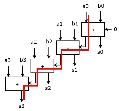
We first introduce a notation to discuss the structure of arithmetic operations. We define an arithmetic circuit as an acyclic graph with inputs x_1, x_2, .., x_n and outputs y_1, y_2, .., y_m. The values y_i are computed from the inputs x_j through a series of operations. The graph contains several nodes representing operations and edges representing data dependencies. The following is an example of an addition of four numbers. The data types of x_i and y_i are application dependent; in the following, we assume that they are unsigned numbers of a given precision.
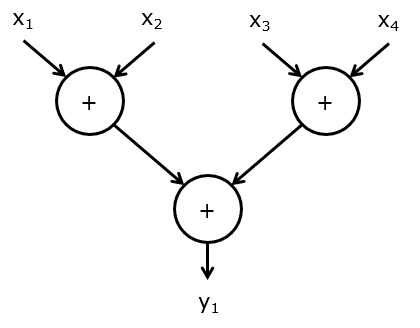
The graph as shown is a functional, maximally parallel specification of operations. The graph shows how y_1 is computed but does not show what hardware is involved. When we think about the concrete implementation of this algorithm, the following elements have to be addressed.
To compute this graph, we will need a hardware module with one or more input ports, output ports, and adders. Deciding the number of operators for an operation is called allocation. For example, for the graph given above, we can allocate a single input port, a single output port, and an adder.
The minimum and maximum number of operators is a design decision. As long as there is at least one operator for every operation, the graph can be computed. Of course, it makes no sense to allocate more operators than operations (of a given type) in the graph, since this extra hardware would not be utilized. Furthermore, one would want to balance the operators. If there are 10 additions for each multiplication, then an architecture with a single adder and a single multiplier will leave the multiplier mostly untouched. Note also, that such a consideration (i.e., operator balancing) only makes sense if you understand or know the application. A CPU, for example, may allocate an adder and a multiplier simply because it needs to be capable of running every possible C program regardless of the operator balance in one specific C program.
All operations have to be scheduled according to a timeline of clock cycles. The schedule of operations needs to be such that we never use more than the number of operators available at that clock cycle. For example, with a single adder module, we can compute only a single addition per clock cycle. Therefore, additional operations cannot be simultaneously scheduled on a single adder.
As a byproduct of the scheduling, we will assign to execution of operations to operators. The assignment is trivial with a single operator, such as a single addition. However, with complex graphs, there may be multiple possible assignments for the scheduled graph. Therefore, your design will have to choose one assignment.
The edges that cross clock cycles will have to store data in a register. The number of registers needed for the execution of a graph depends on the number of live signals/variables.
The following shows one possible schedule with a register assignment. In the example schedule, the IN and OUT operations are added to express the use of the input port resp. output port. There are many possible schedules that meet the data dependency constraint: an operation cannot execute before its operands are available.
The right of the figure illustrates the assignment of signals to registers. Registers can be reused when they no longer have to store a signal. For example, signal x1 is written into R1 in clock cycle 1, and read out of R1 in clock cycle 3. Register R1 is thus available from cycle 3 to store new data, and it is overwritten with the addition result. This register allocation technique, which will greedily allocate the first available register to hold a new result, is called a left-edge assignment.
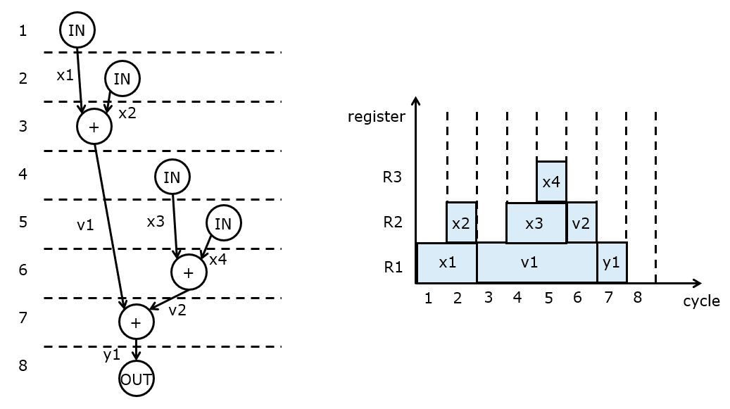
Once we have the scheduling and assignment solved, it’s easy to write a table with register transfers that capture the implementation.
Cycle 1:   R1  <- IN
Cycle 2:   R2  <- IN
Cycle 3:   R1  <- R1 + R2
Cycle 4:   R2  <- IN
Cycle 5:   R3  <- IN
Cycle 6:   R2  <- R3 + R2
Cycle 7:   R1  <- R1 + R2
Cycle 8:   OUT <- R1
When operators’ allocation changes, the schedule can also change. For example, let’s assume we have two input ports. Then we can optimize the schedule as follows. This schedule has almost full utilization of the adder; the utilization would become 100% if we’d allow the input operation and the output operation to execute in the same cycle with the adder.
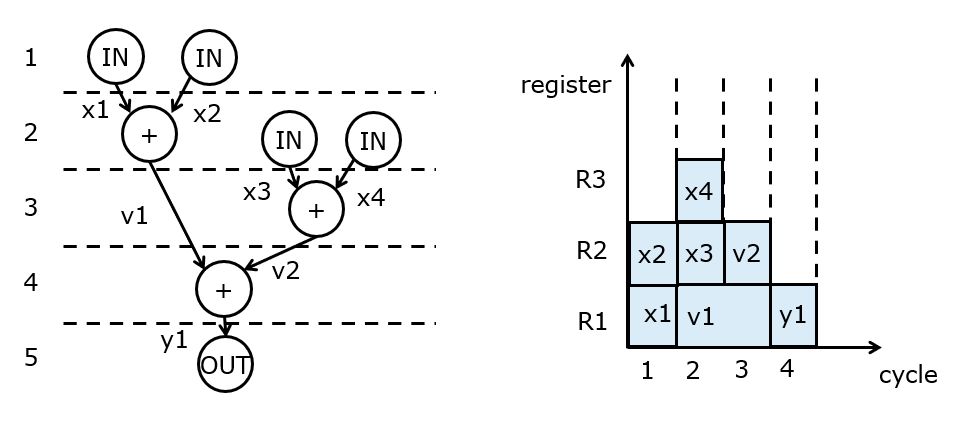
From this schedule, we can derive the following RTL.
Cycle 1:   R1  <- IN1; R2 <- IN2
Cycle 2:   R1  <- R1 + R2; R2 <- IN1; R3 <- IN2
Cycle 3:   R2  <- R2 + R3
Cycle 4:   R1  <- R1 + R2
Cycle 5:   OUT <- R1
Finding good scheduling and assignment is an optimization problem that has been extensively investigated. See, e.g. Gajski, Dutt, Wu, Lin, High Level Synthesis.
The scheduling and assignment also work when the algorithm has state variables (ie. variables that store algorithm state in between successive inputs). In that case, the state variables are treated as internal inputs and outputs of the graph. These state variables provide outputs in the first clock cycle and accept new information in the last clock cycle. The following example computes a running sum of the last three inputs. The input graph is shown at the top of the figure. This graph contains two state variables, T1 and T2. The algorithm computes X + T1 + T2. Then, T1 is copied into T2, X is copied into T1, a new X is read, and the next output Y is computed.
The lower left of the figure shows a schedule assuming a single input port, a single output port, and a single adder. The entire graph can be computed in four clock cycles. In the fourth clock cycle, the output is written. Simultaneously, the state variables T1 and T2 are updated for the next iteration of the algorithm.
The lower right of the figure shows a register assignment. Besides two registers, R1 and R2 to hold the state variables, two additional registers R3 and R4 are needed. Note that R3, holding the input x1, cannot be overwritten after a single clock cycle because this value is written into T1 at the end of the schedule.
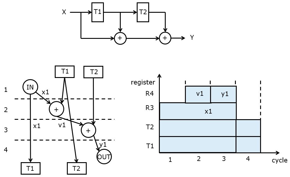
The RTL of this algorithm looks as follows.
Cycle 1: R3 <- IN
Cycle 2: R4 <- R3 + T1
Cycle 3: R4 <- R4 + T2
Cycle 4: OUT <- R4; T2 <- T1; T1 <- R3
Even though we have discussed scheduling, allocation and assignment in the context of mapping arithmetic expressions to hardware, it’s clear that these design techniques apply to a wide variety of design tasks. In fact, they are the core operations of high level synthesis, which aims to turn (imperative) C programs to (parallel) RTL descriptions.
Bit-Serial Design
Attention
The examples discussed in this section are available on https://github.com/wpi-ece574-f22/ex-arithmetic
Arithmetic operations have a great deal of natural regularity and parallelism. An expression such as
wire [0:1023] a, b, c;
assign c = a + b;
consists in fact of 1023 single-bit additions. A traditional, straightforward implementation of such an adder is to define a full-adder module.
module fulladd(input wire a, input wire b, input wire cin,
               output wire sum, output wire cout);
      assign sum  = a ^ b ^ cin;
      assign cout = (a & b) | (b & cin) | (cin & a);
endmodule
And then instantiate a chain of these full adder modules to create the wordlength required.
module add4(
   input logic [3:0] a,
   input logic [3:0] b,
   output logic [3:0] sum,
   output logic cout
);

   logic [3:0] ci, co;
   fulladd A [3:0] (.a(a), .b(b), .ci(ci), .sum(sum), .co(co));
   assign ci[3:1] = co[2:0];
   assign ci[0]   = 1'b0;
   assign cout    = co[3];

endmodule
This design becomes slower the longer the operands become, because the ripple carry chain runs through all the adder modules.

A digit-serial or bit-serial design is an implementation technique that strips down the arithmetic operation to its elementary steps, and then schedules these steps sequentially. For example, in a bit-serial adder, rather than adding all input bits at once, we will add only two bits at a time, implementing just a single full-add operation every clock cycle.
module serialadd(
   input logic a,
   input logic b,
   output logic s,
   input logic sync,
   input logic clk
);

   logic carry, q;

   always_ff @(posedge clk)
   begin
      if (sync)
      begin
         carry <= 1'b0;
         q     <= 1'b0;
      end
      else
      begin
         q     <= a ^ b ^ carry;
         carry <= (a & b) | (b & carry) | (carry & a);
      end
   end

   assign s = q;

endmodule
This bit-serial adder design can perform an N-bit addition in N clock cycle while requiring only one full-adder data path. Bit-serial design is a popular technique when the hardware clock frequency is much higher than the word-level data rate. For example, in digital audio, digital samples are tens of KHz (say, 48 KHz), while the digital ICs can easily run at 20MHz, leaving 416 clock cycles of processing for every sample. Therefore, rather than implementing DSP operations (multiply, add, ..) at word-level, it is more efficient to implement these operations in a bit-serial manner.
The bit-serial design has several important advantages.
First, there is a drastic reduction of logic, especially at longer wordlengths. For short wordlength, the gain becomes proportionally smaller.
Bit-serial design needs fewer wires, as it reuses logic gates and wiring to those gates. Especially when the input and output data format to a bit-serial design is in a bit-serial manner as well, the system interconnect becomes much smaller, reducing from N data wires to 1 data wire and a sync wire.
Bit-serial design has a short critical path because it completes only a single bit operation in a clock cycle.
Bit-serial design brings some disadvantages too, however.
Bit-serial designs need to run at a much higher clock frequency compared to an equivalent bit-parallel design. This works well for the case of audio digital signal processing, but it’s easy to see that there are many applications where bit-serial design does not apply.
Bit-serial designs need to manage a control signal, sync, for every operation. In a complex design (i.e. a complex operation graph), maintaining synchronization among different operations can be challenging.
Bit-serial designs introduce extra storage needed to remember to carry bits and other intermediate results.
Bit-serial computation applies not only to individual operations but also to entire algorithms. For example, the following is a bit-serial design of the adder three we discussed before. Initially, four words are converted from parallel to bit-serial format and added using three bit-serial addition modules. At the end, the output is converted back to parallel format. The sync signal is a pulse that is high for 1 cycle every N cycles, with N the bit-parallel wordlength. In between levels, the sync signal is delayed for one cycle. That is because a bit-serial operation introduces a latency of one clock cycle: if the LSB is fed into the input of a bit-serial module at cycle 0 mod N, then the LSB of the output will be read at cycle 1 mod N.
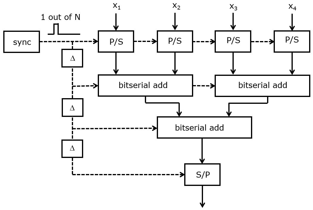
The P/S and S/P module perform parallel to serial, and serial to parallel conversions.
Attention
The Verilog code shown below can be found on https://github.com/wpi-ece574-f23/ex-arithmetic
module topadd(
   input logic [7:0] a,
   input logic [7:0] b,
   input logic [7:0] c,
   input logic [7:0] d,
   output logic [7:0] q,
   input logic clk,
   input logic rst
);

   logic [7:0] ctl;

   logic ctl0, ctl1, ctl2, ctl3;

   always_ff @(posedge clk or posedge rst)
   begin
      if (rst)
         ctl <= 8'b1;
      else
         ctl <= {ctl[6:0], ctl[7]};
   end

   assign ctl0 = ctl[0];
   assign ctl1 = ctl[1];
   assign ctl2 = ctl[2];
   assign ctl3 = ctl[3];

   logic as, bs, cs, ds, abs, cds, sums;

   ps ps1(a, ctl0, clk, as);
   ps ps2(b, ctl0, clk, bs);
   ps ps3(c, ctl0, clk, cs);
   ps ps4(d, ctl0, clk, ds);

   serialadd a1(
      .a(as),
      .b(bs),
      .s(abs),
      .sync(ctl1),
      .clk(clk)
   );

   serialadd a2(
      .a(cs),
      .b(ds),
      .s(cds),
      .sync(ctl1),
      .clk(clk)
   );

   serialadd a3(
      .a(abs),
      .b(cds),
      .s(sums),
      .sync(ctl2),
      .clk(clk)
   );

   sp sp1(
      .a(sums),
      .s(q),
      .sync(ctl3),
      .clk(clk)
   );

endmodule
Running the bitserialadd example
On the class design server, you can run and synthesize this example as follows.
First, check out the repository, and move to the bitserialadd example.
git clone https://github.com/wpi-ece574-f23/ex-arithmetic
cd bitserialadd
There are four subdirectories which will be familiar from earlier lectures.
|
Design files |
|
Synthesis design constraints |
|
Testbench and simulation subdirectory |
|
Synthesis subdirectory |
Simulation is driven by Xcelium.
cd sim
make
The simulation testbench will add the numbers 1, 2, 3 and 4 and print the result every 8 clock cycles (as it takes 8 clock cycles to compute a result). You’ll note that the first output is X (unknown). Think about why that would happen … you can answer it later.
You can also run synthesis on the bitserial adder.
cd syn
make
To understand what the synthesis is doing, study the makefile and the genus_script.tcl. The makefile describes the inputs to the synthesis. We implement the bitserial adder on a 2ns clock for 130nm standard cells. Note how VERILOG can be used to specific multiple (hierarchical) Verilog files. The genus_script.tcl needs no modification unless you want to change the synthesis constraints, which are initially hardcoded to ../constraints/constraints_clk.sdc.
syn:
        BASENAME=bsadd \
                CLOCKPERIOD=2 \
                TIMINGPATH=/opt/skywater/libraries/sky130_fd_sc_hd/latest/timing \
                TIMINGLIB=sky130_fd_sc_hd__ss_100C_1v60.lib \
                VERILOG='../rtl/ps.sv  ../rtl/serialadd.sv  ../rtl/sp.sv  ../rtl/topadd.sv' \
                genus -f genus_script.tcl
The outputs of the synthesis are collected in the outputs and reports directory.
The bitserial adder requires 93 cells and measures 1498 sqm. It has a 50 picosecond slack which means that it’ll run at the specified 500MHz (at least, in synthesis). Finally, it consumes 1.13mW of power when run at 500Mhz. All these numbers can be extracted from the reports. The relevant sections are reproduced below.
# cat bsadd_report_area.rpt

  ...
Instance Module  Cell Count  Cell Area  Net Area   Total Area   Wireload
--------------------------------------------------------------------------
topadd                   93   1497.686     0.000     1497.686 <none> (D)
  ...

# cat bsadd_report_timing.rpt

  ...
             Setup:-     151
     Required Time:=    1849
      Launch Clock:-       0
         Data Path:-    1798
             Slack:=      50
  ...


# cat bsadd_report_power.rpt

  ...
  -------------------------------------------------------------------------
    Category         Leakage     Internal    Switching        Total    Row%
  -------------------------------------------------------------------------
      memory     0.00000e+00  0.00000e+00  0.00000e+00  0.00000e+00   0.00%
    register     8.12842e-07  9.59860e-04  2.74165e-05  9.88089e-04  87.11%
       latch     0.00000e+00  0.00000e+00  0.00000e+00  0.00000e+00   0.00%
       logic     1.45033e-07  1.97308e-05  1.22465e-05  3.21223e-05   2.83%
        bbox     0.00000e+00  0.00000e+00  0.00000e+00  0.00000e+00   0.00%
       clock     0.00000e+00  0.00000e+00  1.14048e-04  1.14048e-04  10.05%
         pad     0.00000e+00  0.00000e+00  0.00000e+00  0.00000e+00   0.00%
          pm     0.00000e+00  0.00000e+00  0.00000e+00  0.00000e+00   0.00%
  -------------------------------------------------------------------------
    Subtotal     9.57874e-07  9.79591e-04  1.53711e-04  1.13426e-03  99.99%
  Percentage           0.08%       86.36%       13.55%      100.00% 100.00%
  -------------------------------------------------------------------------
  ...
Multiplication
Multipliers have interesting bit-serial designs, too. A multiplier is an operation with quadratic complexity: every bit in operand 1 has to touch every bit in operand 2. So, for example, the product of two four-bit numbers, 1101 and 1011, would look as follows.
        1 0 1 1     1  (lsb)
      1 0 1 1       1
    0 0 0 0         0
  1 0 1 1           1
---------------
0 1 1 1 1 0 0 1
There is a high regularity in this operation. At the bit level, a multiplication is just an AND operation. The challenge of implementing the multiplication then, is to add all partial products together. We define an elementary multiplier bitcell as a single-bit multiplication (AND) and an accumulator that will add the partial product to the running sum.
module bitmuladd(input wire a,    // a operand
                 input wire b,    // b operand
                 input wire ci,   // carry in
                 input wire si,   // sum in
                 output wire co,  // carry out
                 output wire so); // sum out

   wire m;

   assign m = a & b;

   assign so = m ^ si ^ ci;
   assign co = (m & si) | (si & ci) | (ci & m);

endmodule
With this bitmuladd, we can create multipliers for an arbitrary-length A and B operand. The following structure performs a four-bit by four-bit multiplication. First, the bits of the B operand are passed vertically down into the multiplier cells. The bits of the A operand are passed across. The resulting structure is a multiplier array for unsigned multiplication.
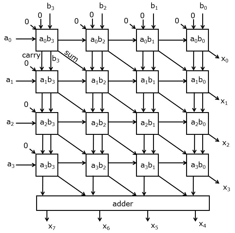
While the Verilog example describes an 8-bit bitserial multiplier, this figure shows a 4-bit multiplier for simplicity.
The bit-serial version of this array multiplier can be made by computing the array row by row, using four parallel bit-serial multiply-accumulate modules.
module serialmuladd (
    input wire a,    // a operand
    input wire b,    // b operand
    input wire clk,
    input wire sync,
    input wire si,   // sum in
    output wire so   // sum out
);

    reg carry;
    reg sum;

    wire m;
    assign m = a & b;

    always_ff @(posedge clk)
        if (sync)
            begin
                sum <= m ^ si;
                carry <= m & si;
            end
        else
            begin
                sum <= m ^ si ^ carry;
                carry <= (m & si) | (si & carry) | (carry & m);
            end

    assign so = sum;

endmodule
Here is an example of an 8x8 bitserial multiplier, which uses eight of the
serialmuladd modules. The a operand is converted into a bitserial
format on 16 bits (not 8 bits). Then, after 8 cycles, the 8 LSB of a*b
start to appear at the S/P output. 8 clock cycles later, all LSB’s (the rows
of the bitmatrix multiplier) have been completed. To extract the 8 MSB’s,
additional work is needed. According to the bitmatrix multiplier design, the
MSB’s are stored in the carries and sums of each column. We extract these
sums and carries by extending the a operand from 8 to 16 bits, and
padding 8 zeroes on the MSB side. Then, the output format to the
serial-to-parallel module becomes a 16-bit serial number.
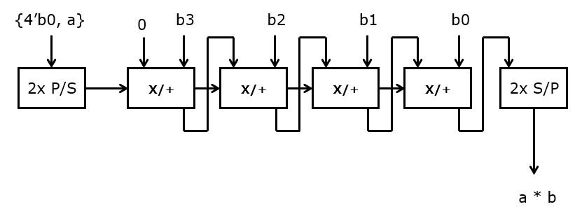
The following shows the top-level configuration of the bitserial multiplier.
Note also how the sync signals are assigned – as ctl0, ctl1, and ctl2. In the first level, there is only a P/S module. In the next level, 8 serialmuladd modules operate in parallel, each time computing one row. In the last level, there is a single S/P module.
module topmul (
    input wire [7:0] a,
    input wire [7:0] b,
    output wire [15:0] q,
    input wire clk,
    input wire rst
);

    reg [15:0] ctl;

    wire ctl0, ctl1, ctl2, ctl3;

    always_ff @(posedge clk)
        if (rst)
            ctl <= 16'b1;
        else
            ctl <= {ctl[14:0], ctl[15]};

    assign ctl0 = ctl[0];
    assign ctl1 = ctl[1];
    assign ctl2 = ctl[2];
    assign ctl3 = ctl[3];

    wire as, qs;
    ps ps1(.a({8'b0, a}), .sync(ctl0), .clk(clk), .as(as));

    wire [7:0] sum;
    assign sum[7] = 1'b0;

    serialmuladd M7(.a(as), .b(b[7]), .clk(clk), .sync(ctl1), .si(sum[7]), .so(sum[6]));
    serialmuladd M6(.a(as), .b(b[6]), .clk(clk), .sync(ctl1), .si(sum[6]), .so(sum[5]));
    serialmuladd M5(.a(as), .b(b[5]), .clk(clk), .sync(ctl1), .si(sum[5]), .so(sum[4]));
    serialmuladd M4(.a(as), .b(b[4]), .clk(clk), .sync(ctl1), .si(sum[4]), .so(sum[3]));
    serialmuladd M3(.a(as), .b(b[3]), .clk(clk), .sync(ctl1), .si(sum[3]), .so(sum[2]));
    serialmuladd M2(.a(as), .b(b[2]), .clk(clk), .sync(ctl1), .si(sum[2]), .so(sum[1]));
    serialmuladd M1(.a(as), .b(b[1]), .clk(clk), .sync(ctl1), .si(sum[1]), .so(sum[0]));
    serialmuladd M0(.a(as), .b(b[0]), .clk(clk), .sync(ctl1), .si(sum[0]), .so(qs));

    sp sp1(.as(qs), .sync(ctl2), .clk(clk), .a(q));

endmodule
Running the bitserialmul example
The bitserialmul example can be run in a similar manner as the bitserial adder.
To simulate, run Xcelium in the sim directory:
cd bitserialmul/sim
make
You should see a result every 16 clock cycles. Again, notice how the two first results are ‘X’ (unknown). Study the source code in rtl and sim, and think about the possible cause.
To map the multiplier to gates, run Genus in the syn directory:
cd bitserialmul/syn
make
Keep in mind that there is a Makefile behind every make that shows exactly what happens.
syn:
        BASENAME=bsmul \
                CLOCKPERIOD=2 \
                TIMINGPATH=/opt/skywater/libraries/sky130_fd_sc_hd/latest/timing \
                TIMINGLIB=sky130_fd_sc_hd__ss_100C_1v60.lib \
                VERILOG='../rtl/ps.sv  ../rtl/serialmuladd.sv  ../rtl/sp.sv  ../rtl/topmul.sv' \
                genus -f genus_script.tcl
Find the area, power and speed of this multiplier and compare it to the bitserial adder implemented previously. Is it 2x, 4x, ..? Can you explain why?
Faster Adder Design
Attention
Refer to the great talk by Teodor-Dumitru Ene on fast adder design for SKY130 https://www.youtube.com/watch?v=P7wjB2DKAIA
After discussing techniques to allocate arithmetic operations on a time axis (scheduling/assignment, bitserial design), we turn our attention to optimizing the performance of arithmetic operations. This means not only minimizing the number of bitoperations but also minimizing the number of levels used in the operand graph so that its critical path (counted as the number of operations from input to output) is as short as possible.
We will discuss the design of fast adder networks as an example. Addition is a prime example of a slow operator when it is mapped using a traditional carry chain.
The basic idea in speeding up this computation, is to compute more operations in parallel by removing data dependencies between them. In the ripple carry adder, bit i cannot be computed until bit i-1 is computed, thereby slowing down the computation. The idea of speeding up addition is to reformulate the computation of the carry bits. With c_i the carry bit at bit i, and s_i the sum bit at bit i, we have:
c_0 &= 0 \\ c_i &= (a_i \& b_i) | (a_i \& c_{i-1}) | (b_i \& c_{i-1}) \\ s_i &= a_i \oplus b_i \oplus c_{i-1}
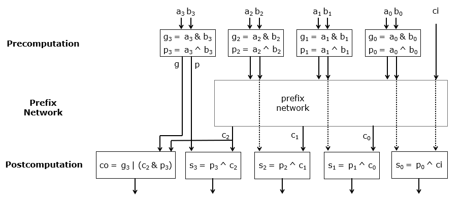
In this expression, c_i depends on c_{i-1}, apparently forcing us to compute all carries one by one. A more efficient scheme there is to express the carry bit in terms of carry-generate and carry-propagate bits:
c_0 &= 0 \\ c_i &= g_i | (p_i \& c_{i-1}) \\ g_i &= a_i \& b_i \\ p_i &= a_i \oplus b_i \\ s_i &= p_i \oplus c_{i-1}
Neither p_i not g_i depends on c_{i-1}, so they can be generated in parallel. The challenge now becomes to compute the c_i for all bits from 0 to i-1.
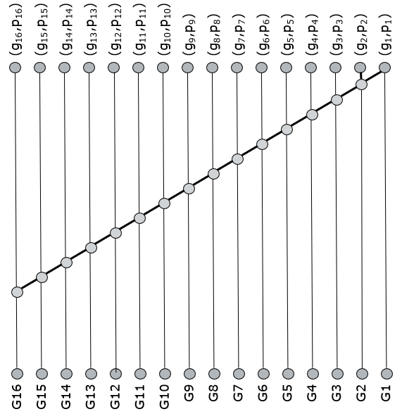
To achieve parallel computation of c_i, we introduce a prefix operation defined as follows.
(g_1, p_1) \bullet (g_2, p_2) = (g_1 | (p_1 \& g_2), p_1 \& p_2)
This prefix operation has two important properties. First, it can compute all c_i using a prefix network.
If we compute
(G_1, P_1) &= (g_1, p_1) \\ (G_2, P_2) &= (g_2, p_2) \bullet (G_1, P_1) \\ (G_3, P_3) &= (g_3, p_3) \bullet (G_2, P_2) \\ (G_4, P_4) &= (g_4, p_4) \bullet (G_3, P_3) \\ ...
then
c_1 = G_1 \\ c_2 = G_2 \\ c_3 = G_3 \\ ...
You can think of (G_i, P_i) as the generate, propagate terms for the sum of all bits with index lower than i. Some authors, including Harris, use the notation (G_{ij}, P_{ij}) to represent the generate, propagate terms for the sum of all bits with index range i down to j. In these notes, we will only use (G_i, P_i).
The second important property is that the \bullet operator is associative.
(g_1, p_1) \bullet [(g_2, p_2) \bullet (g_3, p_3)] = [(g_1, p_1) \bullet (g_2, p_2)] \bullet (g_3, p_3)
Both properties are derived in the paper by Brent & Kung (see reading). The associative property, in particular, is potent. It implies that the prefix operation can be completed in any order. This includes a parallel formulation as a tree operation.
Before discussing the efficient computation of all (G_i, P_i), we first discuss why these terms are useful and lead to faster addition. Since they lead to computation of any carry bit c_i, we have a way to quickly compute the sum bit. Indeed, the sum bit is directly computed as s_i = p_i \oplus c_{i-1}, as we have derived earlier. Furthermore, the most-significant carry-output bit is given by c_i = g_i | (p_i \& c_{i-1}).
The adder can thus be broken down in three parts: a precomputation part, a prefix network, and a post-computation part. The precomputation part generates all the (g_i, p_i) terms in parallel from the inputs (a_i,b_i). The prefix network generates all the (G_i, P_i) terms. And the post-computation part generates the final sum bits and the carry-output bit for the overall adder. The pre-computation and post-computation contains only a single level of logic (assuming you don’t need the final carry-out bit). The delay of the overall adder thus is strongly dependent on the delay of the prefix network.
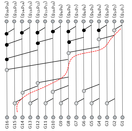
Prefix Trees
Prefix trees are a way to efficiently compute all (G_i, P_i) needed for the prefix tree outputs.
Assume that we now need to compute the most significant carry bit using the prefix tree. Assuming a 16-bit addition, we will implement a prefix three as follows. Recall the complexity of the \bullet: it’s an AND operation and an OR-AND operation. In a standard-cell library, OR-AND gates are available as primitive cells. Thus, every \bullet corresponds to two cells.
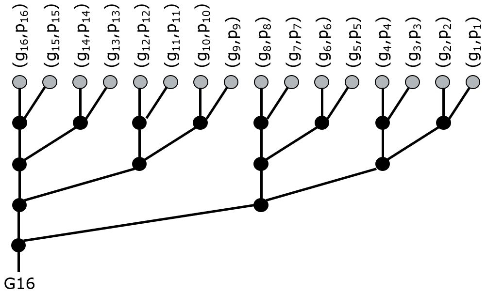
Clearly, the carry bit of bit 16 of a 16-bit adder can be computed using 4 levels of the prefix operation \bullet. Of course, to compute all sum bits, we need to know all carry bits (the full prefix tree), not just the most significant one. However, it turns out that all carry bits are available using just a few additional prefix operations arranged in an inverted tree.
The critical path in this tree runs through G15, which requires 7 prefix operations. This broadcasting increases the fanout of logic within the prefix tree (the fanout is the number of gates that are driven with a given gate). A high fanout may possibly slow down the computation of the carry chain.
However, there are other ways to implement a prefix carry chain, including solutions that don’t crank up the fanout. Let’s first consider the minimum design requirements. We know that the number of logic levels to add up N pairs of numbers is log_2(N). That is because we can express the addition as a parallel tree of additions: first add all pairs of numbers, than add all pairs of pairs to form quadrupples, then add all quadruples, and so forth. Thus, the minimum number of logic levels for an N-bit adder is log_2(N).
Now, it’s certainly possible to do much worse than that. Consider, for example, a serial addition. It computes every G_i sequentially from the lowest to the highest index. That design uses an AND-OR operation at every grey node, and the critical path runs through every node. The grey node is a simplified version of the prefix operation (\bullet) defined earlier.
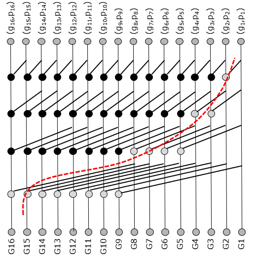
So, improved implementations of the prefix network have to exploit parallelism. Below is the example of the Brent-Kung tree. This is certainly a faster than a pure serial solution. To compute G15, for example, we now have to cross 6 logic levels. Nice, but not optimal.
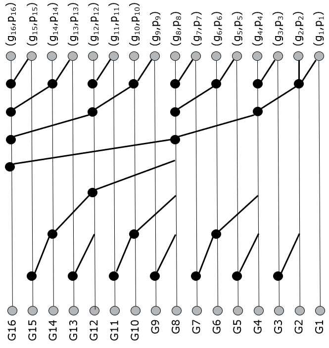
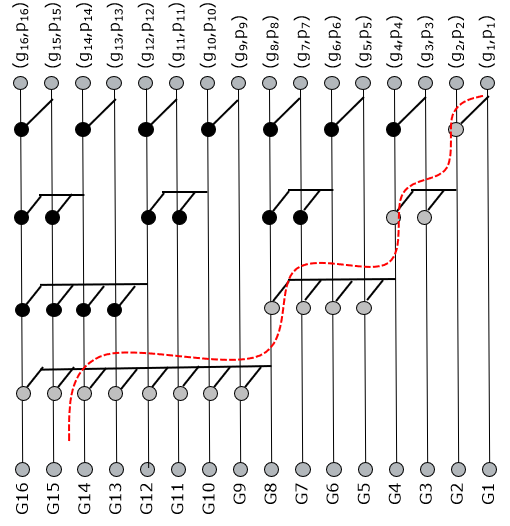
A faster solution is the Kogge-Stone tree, which aims at a maximally parallel implementation. Indeed, the following tree for a 16-bit adder can compute every carry using only four levels of prefix logic. However, Kogge-Stones trees create a dense wiring pattern which, in the end, will also hurt performance and placement density.
An alternate solution is the Sklansky tree, which avoids a dense wiring pattern by broadcasting the intermediate results of the prefix computation to many different places in the tree. The Sklansky tree has the same optimality of four logic levels. However, because it broadcasts the intermediate results, several gates will have a high fanout. This, in the end, may also become a bottleneck in high-speed implementation.
Building and testing prefix trees
You can do a quick handson using the code provided in the repository for this lecture.
This has to be done in the exploration directory.
To complete the handson, you have to download Teodor-Dumitru Ene’s repository with prefix-adder tree generators. He wrote a python package that creates adders of a selected width using a parametrizable topology (Brent-Kung, Kogge-Stone, Sklanksy, Serial). Download and install the Python package on your class account as follows.
git clone git@github.com:tdene/synth_opt_adders.git
cd synth_opt_adders
pip3 install --upgrade pptrees
Next, you can generate the Verilog code for a given adder. For example, an 8-bit Kogge-Stone adder is created with the following Python code.
from pptrees.AdderForest import AdderForest as forest

width = 8
f = forest(width, alias = "kogge-stone")
f.hdl("adder8_koggestone.v")
Once you are able to generate Verilog code, it’s time for a design space exploration. The question is as follows.
Attention
Generate code for an 8-bit adder using four different carry chain architectures: Kogge-Stone, Brent-Kung, Sklansky, and ripple carry.
Map this code using 130nm standard cells (Library sky130_fd_sc_hd__ss_100C_1v60.lib)
and for a clock frequency of 500MHz and 1GHz. Compare the timing performance, area
and power for each solution. Make sure than no design experiences negative slack (timing failure).
Which solution is worst/best in terms of Power? Which solution is worst/best in terms of Area?
To help you get started, a simplified (RTL) adder is already set up under exploration.
You can simulate and implement that RTL variant as follows.
cd exploration/sim
make

cd exploration/syn
make
Note that the synthesis is run two times, for different clock constraints. When the synthesis is complete, read the report files and extract the proper data for this RTL version.
To use the simulation/synthesis flow on your generated adders (Brent-Kung, Kogge-Stone, Sklansky, ripple-carry), you have to copy your code into the rtl directory and make appropriate changes to the makefiles in simulation and synthesis.
Tensor Processing Unit
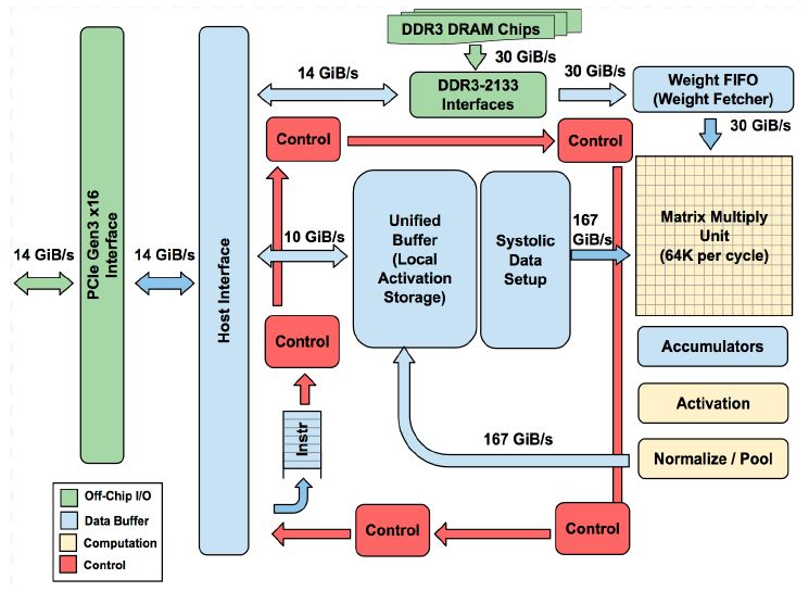
Finally, we will discuss an example how the arithmetic needs of modern processing workloads can affect computer architecture in a big way. Google is using an additional accelerator, called a Tensor Processing Unit, in the servers of its could. The accelerator is used for machine learning applications - first, for inference, but in more recent versions of the chip, also for training.
The paper by Jouppi and his colleagues observes that the need for a TPU became clear when they calculated that people (say, the average user) doing voice search for 3 minutes per day would double the computational demands from data centers to satisfy the matching. Thus they came up with a chip that could prevent this computational performance crisis. This chip, the Tensor Processing Unit, is specialized in matrix multiplications of short data types (8-bit). The chip has an interesting architecture that exploits the massive parallelism available from hardware. The TPUv1 contains 64K multiply-accumulate modules arranged in a 256x256 matrix.
The TPU processor adopts an architecture known as a systolic array.
It is capable of doing massive parallel computations. At full utilization,
the TPU will compute 64K MAC operations per cycle. We explain the main
operation performed by the TPU, a matrix multiplication, through the example
of an 3-by-3 matrix multiplication. That is, we wish to compute the following
operation. The x matrix is input data, the w matrix holds weights, and the
y matrix is output data.
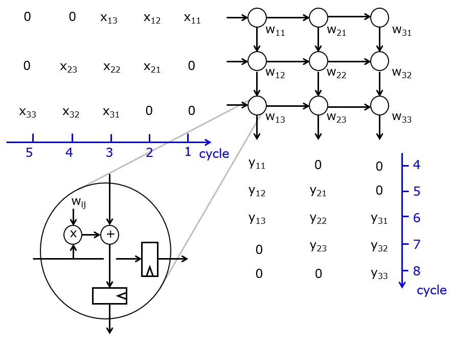
\begin{bmatrix} x_{11} & x_{12} & x_{13}\\ x_{21} & x_{22} & x_{23}\\ x_{31} & x_{32} & x_{33} \end{bmatrix} \times \begin{bmatrix} w_{11} & w_{12} & w_{13}\\ w_{21} & w_{22} & w_{23}\\ w_{31} & w_{32} & w_{33} \end{bmatrix} = \begin{bmatrix} y_{11} & y_{12} & y_{13}\\ y_{21} & y_{22} & y_{23}\\ y_{31} & y_{32} & y_{33} \end{bmatrix}
The systolic array multiplier for this operation holds 9 MAC units arranged in three rows of three columns. Initially, the weights are distributed over the MAC units so each MAC holds on weight. Then, the input data is moved across while the output data is streamed out at the bottom. Note that both input and output data appear in slanted matrices. This accounts for data latency inside of the systolic structure. A single MAC element is shown in the bottom left of the figure. All outputs are computed with a single cycle of latency. However, this structure can deliver massive computational throughput.
This matrix multiplier is central to the TPU’s architecture. In addition, the chip implements an instruction set that helps the programmer to think of the entire matrix multiplication as a single atomic operation.
Google TPUv1 [Jouppi et al, ISCA 2017]
The specialized structure, combined with the specialized arithmetic, implies that the TPU significantly outperforms CPUs and GPUs. For example, table 2 in Jouppi’s paper shows that the design not only consumes lower power, but delivers 30-50x the performance of dedicated CPU/GPU solutions.
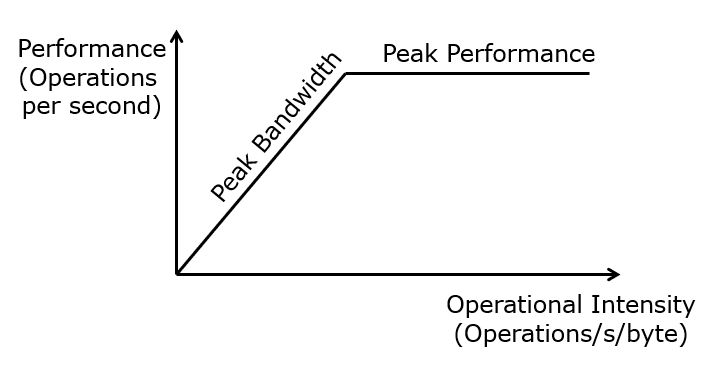
The paper further presents roofline plots of the benchmarks. A roofline plot helps a computer engineer to understand is and architecture is compute bound or memory bound. A roofline plot sets operational intensity (measured in Operations per second per byte) against the performance (measured in Operations per second). Indeed, as fewer operations have to be performed for each fresh data element transported over the memory hierarchy, the demands on the memory I/O bandwidth start to increase, until the point where the memory bandwidth is the main bottleneck. The Benchmarking of the TPU analysis shows that the first version of the TPU (2017) is limited by the memory bottleneck and not by the computational bottleneck, for 6 different machine learning benchmarks. As of this writing, Google has produced two new versions of the TPU. All of them still use the matrix multiplier as the central computational element, while optimizing the interconnect and on-chip memory towards the multiplier.