Attention
This document was last updated Aug 22 24 at 21:58
Full-chip layout
Important
The purpose of this lecture is as follows.
To describe the concept of padcells and their integration in the IC design flow
To clarify the purpose of hard macros
To describe the integration of hard macros in the IC design flow
To explain the concept of scan testing in chip design
To describe the integration of scan chains in the IC design flow
To explain the advantages of latches in high-performance design
Important
The examples discussed in this lecture are available from https://github.com/wpi-ece574-f23/ex-finishing
Attention
The following references are relevant background to this lecture.
David G. Chinnery, Kurt Keutzer: Closing the Gap Between ASIC and Custom - Tools and Techniques for High-Performance ASIC Design. Springer 2004, ISBN 978-1-4020-7113-3, pp. I-XIV, 1-414.
Important
This is the last lecture before we kick off the project. In this lecture, we will close several open threads and show how you can create a floorplan for a complete chip. This require to address several different items that are only loosely related. The objective of the lecture, however, is to prepare you with sufficient tools and know-how so that you can succesfully complete the project.
Input/Outpad Pad Frame
A crucial element in the chip design process is the integration of the chip die in a package. Indeed, many physical performance factors of a chip are directly dependeing on the chip package, such as signal I/O bandwidth and maximum power consumption. Chip package design enginering is, in fact, a specialization in its own right.
From the chip design perspective, there are two major strategies to enable connectvity. The traditional strategy relies in wire bonding, which involves the connecting a bond wire between the chip and the chip package. In this strategy, the contact pads are arranged around the die. More recent technologies use flip chip bonding to enable a higher density. In this case the die is flipped and attached onto a package substrate that directly connects to the chip using small conductive bumps. The connection pads can now be distributed throughout the die.
Attention
In this lecture, we will not discuss packaging technology itself - although this is arguably an area of intense research and development. Here are some references to explore further, in case you’re interested in the specific aspect of chip packaging.
Ho-Ming Tong, Yi-Shao Lai, C.P. Wong, “Advanced Flip Chip Packaging,” Springer 2013, 978-1-4419-5768-9
Douglas Yu, “TSMC Packaging Technologies for Chiplets and 3D,” HotChips 2021, online presentation
Ravi Mahajan, Sandeep Sane, “Advanced Packaging Technologies for Heterogeneous Integration,” HotChips 2021, online presentation
Chengjie Xie, Alonso Conejos Lopez, “Packaging Technology,” University of Florida (Navid Asadi), Online Presentation, part 1, part 2, part 3, part 4, part 5
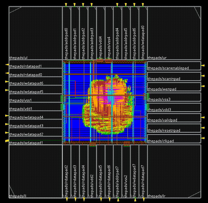
This lecture only covers the design of padframes for digital circuits. The following figure demonstrates the structure of a chip for wire-bonding. The core area with power mesh is surrounded by ring containing IO padcells and corner cells. The main function of padcells is to amplify the tiny signal (current-wise) from on-chip to a signal that is suitable to drive an IO pin of a chip. An IO padcell also provides a bonding area where a wire (in the case of a flip-chip, a solder bump) can be attached. IO pads will handle voltage level conversion when the input/output voltage is different from the core voltage. IO pads also protect the core from Electrostatic Discharge by a pair of reverse-biased diodes between VSS and the pad, and the pad and VDD.
Additional corner cells are placed on the IO ring as well, to ensure that the padring power infrastructure is fully closed. In a typical chip, multiple power pads (VDD/VSS) are available. The redundant power pads ensure an even distribution of power over the chip and ensure that all areas of the power mesh maintain nominal voltage.
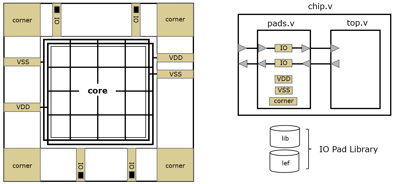
In Verilog, the top-level of a chip is implemented as the interconnection of a pad frame and the top cell of the design. The pad frame instantiates the padcells and provides a dummy connectivity to a new top level chip.v. This hierarchy ensures that the design can be simulated and analyzed including the pad cells. The pad cells are treated as a block box in Verilog; they do not have a behavioral description (apart from a trivial interconnection) but their type name matches that of a similar cell in the IO design library. To design a pad frame, we need at least two views of the IO design library: a timing view (lib) and a layout view (lef).
To design a padring on an IC, we must therefore implement the following structures.
A top-level padframe to interconnects top-level pins and chip-level pins, by instantiating IO padcells. In addition, the padframe must instantiate power pads (VDD, VSS) and corner pads.
A chip IO description that specifies the spatial ordering and arrangement of the padcells.
The following is the example of a padring design for the moving average filter. The example can be downloaded from https://github.com/wpi-ece574-f23/ex-finishing. First, recall the top-level interconnect of mavg. The design has 6 input pins, and 4 output pins.
module mavg(
 input logic [3:0] x,
 output logic [3:0] y,
 input logic reset,
 input logic clk
);
We now implement a padframe that allocates 6 input padcells, 4 output padcells, and 4 pairs of power padcells. The chip-level description illustrates the interconnect between the top and the chip pins. Note how pads has an input pin and an output pin for each single pad.
module chip(
            input wire  clk,
            input wire  reset,
            input wire  x0,
            input wire  x1,
            input wire  x2,
            input wire  x3,
            output wire y0,
            output wire y1,
            output wire y2,
            output wire y3);

   wire                 die_clk;
   wire                 die_reset;
   wire [3:0]           die_x;
   wire [3:0]           die_y;

   pads thepads(.clk(clk),
                .reset(reset),
                .x0(x0),
                .x1(x1),
                .x2(x2),
                .x3(x3),
                .y0(y0),
                .y1(y1),
                .y2(y2),
                .y3(y3),
                .die_clk(die_clk),
                .die_reset(die_reset),
                .die_x(die_x),
                .die_y(die_y));

   mavg thecore(.x(die_x),
                .y(die_y),
                .reset(die_reset),
                .clk(die_clk));

endmodule
The pads description instantiates all padcells including the power pads. PADI is an input padcell, PADO is an output padcell, and PADCORNER, PADVDD1, PADVSS1 are corner, VDD and VSS respectively. The names of padcells are library specific, and thus can be different for a different technology.
module pads(
            input wire        clk,
            input wire        reset,
            input wire        x0,
            input wire        x1,
            input wire        x2,
            input wire        x3,
            output wire       y0,
            output wire       y1,
            output wire       y2,
            output wire       y3,

            output wire       die_clk,
            output wire       die_reset,
            output wire [3:0] die_x,
            input wire [3:0]  die_y);

   PADI clkpad(.PAD(clk), .OUT(die_clk));
   PADI resetpad(.PAD(reset), .OUT(die_reset));

   PADI x0pad(.PAD(x0), .OUT(die_x[0]));
   PADI x1pad(.PAD(x1), .OUT(die_x[1]));
   PADI x2pad(.PAD(x2), .OUT(die_x[2]));
   PADI x3pad(.PAD(x3), .OUT(die_x[3]));

   PADO y0pad(.IN(die_y[0]), .PAD(y0));
   PADO y1pad(.IN(die_y[1]), .PAD(y1));
   PADO y2pad(.IN(die_y[2]), .PAD(y2));
   PADO y3pad(.IN(die_y[3]), .PAD(y3));

   PADCORNER ul();
   PADCORNER ur();
   PADCORNER ll();
   PADCORNER lr();

   PADVDD1 vdd1();
   PADVDD1 vdd2();
   PADVDD1 vdd3();
   PADVDD1 vdd4();

   PADVSS1 vss1();
   PADVSS1 vss2();
   PADVSS1 vss3();
   PADVSS1 vss4();

endmodule

module PADI(input wire PAD, output wire OUT);
   assign OUT = PAD;
endmodule

module PADO(output wire PAD, input wire IN);
   assign PAD = IN;
endmodule

module PADVSS1();
endmodule

module PADVDD1();
endmodule

module PADCORNER();
endmodule
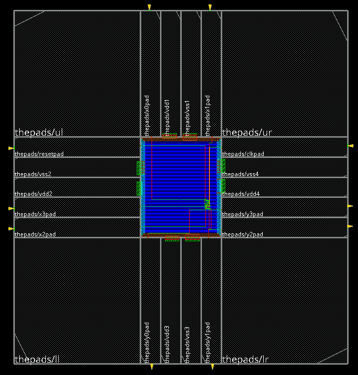
The Verilog description only reflects the connectivity. The spatial arrangement of the padcells is captured in a different format, similar to the format we used to describe the placement of IO pins in the layout of modules. Consider the following example, which arranges a total of 18 pads (10 IO and 8 power) around the chip.
(globals
  version = 3
  io_order = default
)
(iopad
    (topright
        (inst name="thepads/ur")
    )
    (top
        (inst name="thepads/x0pad")
        (inst name="thepads/vdd1")
        (inst name="thepads/vss1")
        (inst name="thepads/x1pad")
    )
    (topleft
        (inst name="thepads/ul")
    )
    (left
        (inst name="thepads/x2pad")
        (inst name="thepads/x3pad")
        (inst name="thepads/vdd2")
        (inst name="thepads/vss2")
        (inst name="thepads/resetpad")
    )
    (bottomleft
        (inst name="thepads/ll")
    )
    (bottom
        (inst name="thepads/y0pad")
        (inst name="thepads/vdd3")
        (inst name="thepads/vss3")
        (inst name="thepads/y1pad")
    )
    (bottomright
        (inst name="thepads/lr")
    )
    (right
        (inst name="thepads/y2pad")
        (inst name="thepads/y3pad")
        (inst name="thepads/vdd4")
        (inst name="thepads/vss4")
        (inst name="thepads/clkpad")
    )
)
After place and route, we obtain the following layout. Notice how the power pads are connected to the VDD/VSS ring around the core of the circuit. The actual design on the chip is tiny compared to the size of the padring – most of the core area remains empty. This is an example of a pad-constrained design, a design where the area needs of the input/output infrastructure outweigh the area needs of the core. The opposite of a pad-constrained design is a core-constrained design. For a detailed discussion of the design flow steps from Verilog to this layout using Cadence tooling, refer to the demonstration in the lecture video.
Integrating Hard Macros
Chip design often calls for the use of dedicated hard macros for functionality that cannot be captured in standard cells. Examples are memory modules and specialized analog and mixed-signal functionality. Hard macros for digital logic are specialized and therefore provide a higher densitity then what can be achieved using standard cells alone.
A hard macro is defined by means of several views to support its integration in a chip design flow. Such views can include:
A behavioral Verilog view (for simulation)
A timing view (for synthesis & STA)
A layout view (for layout)
Hard macros are the result of manual design or module generators. Such a module generator is a software program that can generate the views for a specific instance of a given module. For example, a RAM generator can generate various RAM modules of different address depth and word size. The use of a RAM generator then allows a chip designer to create exactly the memory configuration required for the design.
We discuss the example of a RAM module integrated in a standard cell design. The RAM is a single-port 128 by 16 bit module, meaning that it can hold 128 words of 16 bits, and that it has a single read/write port. We instantiate this RAM in a system that adds a single level of pipelining at the data output of the RAM.
The following is the top-level RTL view of the system that holds the RAM.
module rampipe(input wire [6:0]   A,
               input wire [15:0]  D,
               input wire         OEN,
               input wire         WEN,
               input wire         CLK,
               output wire [15:0] Q);

   wire [15:0]                    pipe_next;
   reg [15:0]                     pipe;

   ram_128x16A ram(.A(A),
                  .D(D),
                  .OEN(OEN),
                  .WEN(WEN),
                  .CLK(CLK),
                  .Q(pipe_next));

   always @(posedge CLK)
     pipe <= pipe_next;

   assign Q = pipe;

endmodule
To simulate this model, a behavioral view for the RAM is required.
This behavioral view is only used for simulation; for synthesis,
ram_128x16A must be treated as a black box. The use of the SIMULATION macro serves as a reminder that this model is not to be
mapped through inference.
module ram_128x16A (A,
                    D,
                    OEN,
                    WEN,
                    CLK,
                    Q);

   input [ 6:0] A;
   input [15:0] D, Q;
   input        OEN, WEN, CLK;

// black-box model for synthesis

`ifdef SIMULATION
   reg [15:0]   memory [0:127];
   reg [15:0]   DATA_OUT;

    always @ (posedge CLK)
    begin
        if (WEN) begin
           memory[A] = D;
        end
       DATA_OUT = memory[A];
    end

   assign Q = OEN ? DATA_OUT : 16'bz;

`endif

endmodule
Indeed, when we consult the gate-level netlist, we find the same RAM module instantiated directly.
module rampipe(A, D, OEN, WEN, CLK, Q);
  input [6:0] A;
  input [15:0] D;
  input OEN, WEN, CLK;
  output [15:0] Q;
  wire [6:0] A;
  wire [15:0] D;
  wire OEN, WEN, CLK;
  wire [15:0] Q;
  wire [15:0] pipe_next;
  ram_128x16A ram(.CLK (CLK), .CEN (1'b0), .OEN (OEN), .WEN (WEN), .A
       (A), .D (D), .Q (pipe_next));
  DFFXL \pipe_reg[8] (.CK (CLK), .D (pipe_next[8]), .Q (Q[8]), .QN
       (UNCONNECTED));
  DFFXL \pipe_reg[1] (.CK (CLK), .D (pipe_next[1]), .Q (Q[1]), .QN
       (UNCONNECTED0));
  ...
Thanks the to timing view, the resulting netlist can still be evaluated for timing. For example, STA reports that the critical path after synthesis runs from the RAM data output to the input of the pipeline register.
Path 1: MET Setup Check with Pin pipe_reg[14]/CK
Endpoint:   pipe_reg[14]/D (v) checked with  leading edge of 'clk'
Beginpoint: ram/Q[14]      (v) triggered by  leading edge of 'clk'
Path Groups: {clk}
Other End Arrival Time          0.000
- Setup                         0.164
+ Phase Shift                   2.000
= Required Time                 1.836
- Arrival Time                  1.802
= Slack Time                    0.034
     Clock Rise Edge                 0.000
     + Clock Network Latency (Ideal) 0.000
     = Beginpoint Arrival Time       0.000
      ---------------------------------------------------------------------
      Instance      Arc               Cell         Delay  Arrival  Required
                                                          Time     Time
      ---------------------------------------------------------------------
      ram           CLK ^             -            -      0.000    0.034
      ram           CLK ^ -> Q[14] v  ram_128x16A  1.802  1.802    1.836
      pipe_reg[14]  D v               DFFXL        0.000  1.802    1.836
      ---------------------------------------------------------------------
Likewise, the timing view of a hard macro may also contain a power model that approximates the static and dynamic power consumption of the macro as a result of activity on its input pins. This enables power simulation of the RTL/gate-level model including the hard macro.
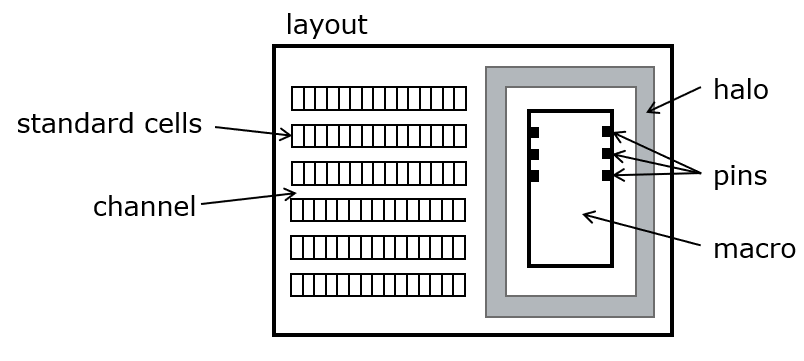
The layout of a design including hard macros requires special care because hard macros require a separate placement and integration. The following considerations must be taken into account.
Hard macros have their own internal power network that must be attached to the chip network. Often, a power ring is added around the macro to make sure power is available anywhere the macro needs to connect to it.
Hard macros have their own pin placement that may not follow the conventional channel interconnect used by standard cells. A halo can be added when placing a hard macro to ensure that every pin can be reached by routing.
Hard macros are typically placed by hand in a position that makes most sense from the interconnect and I/O perspective. Often, this results in a location around the die periphery.
For a detailed discussion of the design process of the layout using Cadence tooling, refer to the demonstration in the lecture video.
Scan Chains for Testable Design
After chip manufacturing, chips are tested to verify that manufacturing defects are absent. The challenge of such a test is that the observability of the chip’s internal logic is limited to the input/output pins. However, merely identifying that a chip is malfunctioning is insufficient. Typically, designers/implementers also want to know where precisely any fault within the chip has occured. If faults consistently occur in the same location of the chip, this may identify a weak aspect of the layout that must be addressed in future iterations.
Scan chains are a common technique to improve the observability of a design. The idea is to arrange every register in the design in a chain, and use a special type of flip-flop with an additional scan-in and scan-out data input.
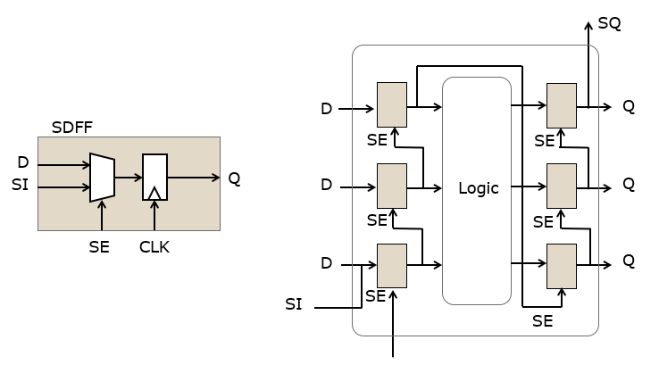
A design with a scan chain makes use of a scan flip-flop (SDFF) which is provided as a separate standard cell. Scan flip-flops are larger than normal flip-flops because of the additional input multiplexer. Hence, a design with a full scan chain (every flip-flop functioning as a scan flip-flop) will be larger/slower than a design with a partial scan chain. On the other side, partial scan will reduce observability.
During synthesis, all scan flip-flops are daisy-chained together into a scan chain. The scan chain allows the insertion of test vectors into the design, where all flip-flops are preloaded with a given value. A single test cycle then allows every flip-flop to be updated, and subsequently the scan chain is read out and the resulting values analyzed.
The objective of test vectors is to identify faults in the logic. Such faults follow a pre-assumed fault model such as stuck-at-1 or stuck-at-0, in which a faulty gate is assumed to output always 1 or always 0. The objective of testing is then to determine, with as few test vectors as possible, if a gate is faulty or not. There are a large number of design parameters to this problem, and test engineering is a specialization in its own right. Some of the considerations include the following.
The observability in the design should be as high as possible. That is, we would want to single out a single faulty gate among all gates in a design. In practice, this coverage may not be achievable, or may only be possible at a tremendous amount of test vectors.
The number of test ports (parallel scan chains) and the length of the test vectors determines the chip testing time, which is a critical cost factor in high-volume products.
The location and number of scan flip-flops in the design determines the efficiency of the testing process. The presence of latches in the design complicates testing because they limit the observability of the gates behind the latch. Latches can be made transparent during scan testing, but this introduces additional design considerations.
Scan testing can be combined with other testing techniques such as built-in self-test (BIST).
Scan chain testing is supported by two separate tools in the chip design process. During synthesis, scan chains are inserted automatically by the synthesis tool. Scan chain insertion determines the order and amount of flip-flops to be converted into scan flops. The result of the synthesis is a list of flip-flops in the scan chain. For example, the following is the result of scan chain insertion in the moving average design. The scan chain contains 259 bits, corresponding to four 64-bit registers and a few state bits of an FSM in the design.
VERSION 5.5 ;
NAMESCASESENSITIVE ON ;
DIVIDERCHAR "/" ;
BUSBITCHARS "[]" ;
DESIGN movavg ;

SCANCHAINS 1 ;
  - top_chain_seg1_clk_rising
    + PARTITION p_clk_rising
      MAXBITS 259
    + START PIN scan_in
    + FLOATING
       acc_reg[0] ( IN SI ) ( OUT Q )
       acc_reg[1] ( IN SI ) ( OUT Q )
       acc_reg[2] ( IN SI ) ( OUT Q )
       acc_reg[3] ( IN SI ) ( OUT Q )
       acc_reg[4] ( IN SI ) ( OUT Q )
       acc_reg[5] ( IN SI ) ( OUT Q )
       acc_reg[6] ( IN SI ) ( OUT Q )
       ...
       tap3_reg[56] ( IN SI ) ( OUT Q )
       tap3_reg[57] ( IN SI ) ( OUT Q )
       tap3_reg[58] ( IN SI ) ( OUT Q )
       tap3_reg[59] ( IN SI ) ( OUT Q )
       tap3_reg[60] ( IN SI ) ( OUT Q )
       tap3_reg[61] ( IN SI ) ( OUT Q )
       tap3_reg[62] ( IN SI ) ( OUT Q )
       tap3_reg[63] ( IN SI ) ( OUT Q )
    + STOP PIN scan_out
;

END SCANCHAINS
END DESIGN
Once the scan chain is in place, a test vector generator will then generate tests that maximize the testing coverage. For example, for the moving average design, 102 test vectors are created which test 25-74 possible faults and which provide 99.99% coverage of all possible faults. The tool also produces a precise estimate of the amount of testing cycles needed to evaluate all test vectors. For a detailed discussion of the design process of the layout using Cadence tooling, refer to the demonstration in the lecture video.
****************************************************************************************************
                           Testmode Statistics: FULLSCAN

                           #Faults      #Tested    #Possibly      #Redund    #Untested  %TCov %ATCov
Total Static                 25076        25074            0            2            0  99.99 100.00
Total Dynamic                30566         4150            0            0        26416  13.58  13.58

                            Global Statistics

                           #Faults      #Tested    #Possibly      #Redund    #Untested  %TCov %ATCov
Total Static                 25076        25074            0            2            0  99.99 100.00
Total Dynamic                32122         4150            0            0        27972  12.92  12.92
****************************************************************************************************


              ----Final Pattern Statistics----

 Test Section Type                       # Test Sequences
----------------------------------------------------------
 Scan                                           1
 Logic                                          102
----------------------------------------------------------
 Total                                          103
Why high-speed design uses latches instead of flip-flops
Although we have avoided the use of latches throughout the course, and always emphasized strictly synchronous design, it helps to explain why design engineers don’t part with latches. In fact, a standard cell library will always have latches available. There are two important reasons for the presence of these latches. First, latches are smaller. Second, it’s possible to design faster circuits with latches due to an technique called time borrowing.
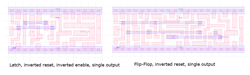
First, latches are smaller than their equivalent flip-flop counterpart. This is apparent when comparing the layout of equivalent functionality. The following figure shows the layout of a Skywater 130nm latch and the a Skywater 130nm flip-flop. Both latches and flip-flops are made out of storage cells which consist of two interters that are feb back on each other. However, a latch needs only a single storage cell, while the flip-flop needs two. Indeed, the need for an edge-triggered clock requires two internal storage cells: one that holds the output when the clock is low, and a second which holds the input when the clock is high. In the case of a latch, only a single one is needed which can be either opened or closed.
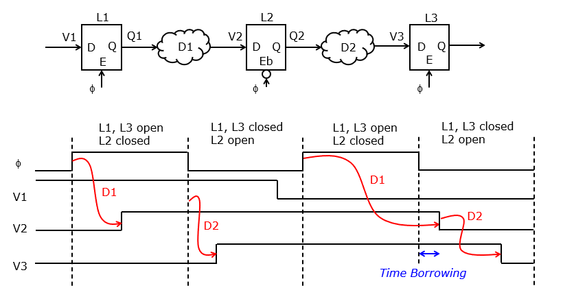
In addition to the area advantage, a latch also enables faster design. The design of circuits with latches requires careful handling of timing, which is out of scope of this lecture. However, a common arrangement found in a resulting latch based design is shown below: portions of logic are separated by latches that open and close on alternate phases of the clock. In this case, L1 and L3 are open when the clock is high, and L2 is open when the clock is low. This alternating pattern when moves data forward into the circuit:
As soon as L1 opens, the value rushes to the output Q1, eventually causing V2 to change. This happens normally before the clock goes low, i.e. before latch L2 opens.
When the clock goes low, L2 propagates the value V2 to Q2. This will cause V3 to change. L3 will not propagate this new input further until the clock goes high again.
The computations happening over D1 and D2 thus take place over a time period that extends over the entire clock cycle (clock high and clock low). The time borrowing effect occurs when the computation of D1 is not finished by the time L2 opens (clock low). This late transition on V2 will be propagate to Q2 and cause a late transition on V3. However, since L3 does not open until the clock goes high again, this delay does not effect overall correctness of the operation. Thus, timing borrowing allows the time needed to compute logic from two levels of logic to be spread over the entire clock cycle. Thus relaxed timing requirement eventually leads to tighter design margins, and thus faster logic.
The full design flow
Finally, we review the overall design flow by means of a complete example, namely a chip for AES encryption/decryption. Let’s first review all stages of the design flow, and the corresponding directory names that we have adopted for our design.
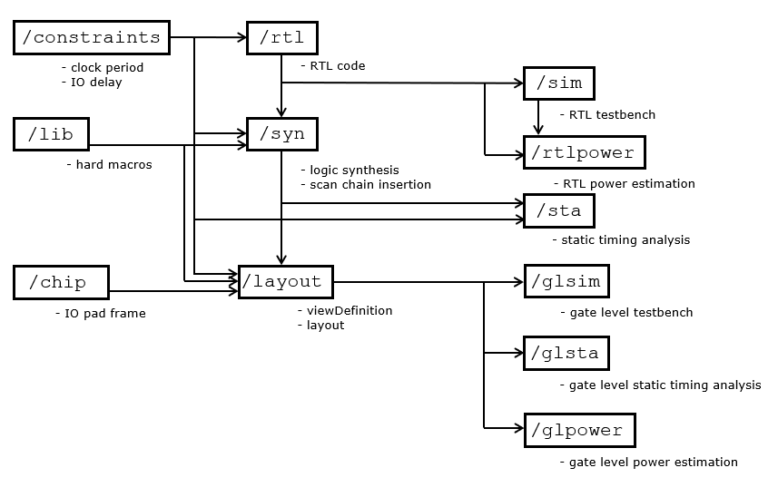
/rtlcontains the register-transfer level code of the design./simcontains the testbench of the design, and possible test-vectors. The design is simulated with Xcelium, and theMakefilemust be properly configured with (System)Verilog file names./constraintscontains the input/output delay constraints and the synthesis clock period of the design in an.sdcfile. The input/output delay constraints can be adjusted by editing this SDC file./syncontains the logic synthesis and test vector generation scripts, used by Genus and Modus respectively. TheMakefilemust be properly configured with synthesis configuration parameters including the technology library. In addition, the synthesis script can be tweaked to modify the optimization level, introduce hard macro’s, etc./rtlpowercontains the RTL power estimation script, which uses the RTL VCD files as well as the RTL source code. TheMakefilemust be properly configured with power estimation parameters, including the number of frames to use (1 to 1000 or twice the number of clock cycles in the VCD, whatever is smaller). Joules estimates power as a graph and a data file./liballocates the behavioral (verilog), timing (lib) and layout (lef) views of any hard macros used in the design./staperforms static timing analysis using Tempus. The STA script needs tuning according to the design parameters./chipdefines the block pin allocation or the padframe of the chip, depending on whether you do a block-level design or a full-chip design./layoutcreates the final layout using Genus and Innovus. TheMakefiledefines relevant design parameters including the libraries to use. The synthesis and layout scripts need manual tuning to enable the use of hard macros and other custom steps./glsimperforms gate-level simulation using the final netlist produced from the design. This final netlist uses delay information (SDF) computed from the layout data./glstaperforms gate-level STA using the final netlist produced from the design using Tempus. The STA uses parasitic information (SPEF) produced from the layout data./glpowerperforms gate-level power esimation using the final netlist produced from the design, and the VCD computed during gate-level simulation.
For a detailed discussion of the design process for the AES chip using Cadence tooling, refer to the demonstration in the lecture video.
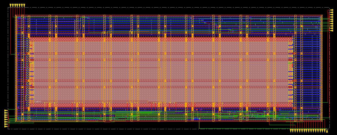
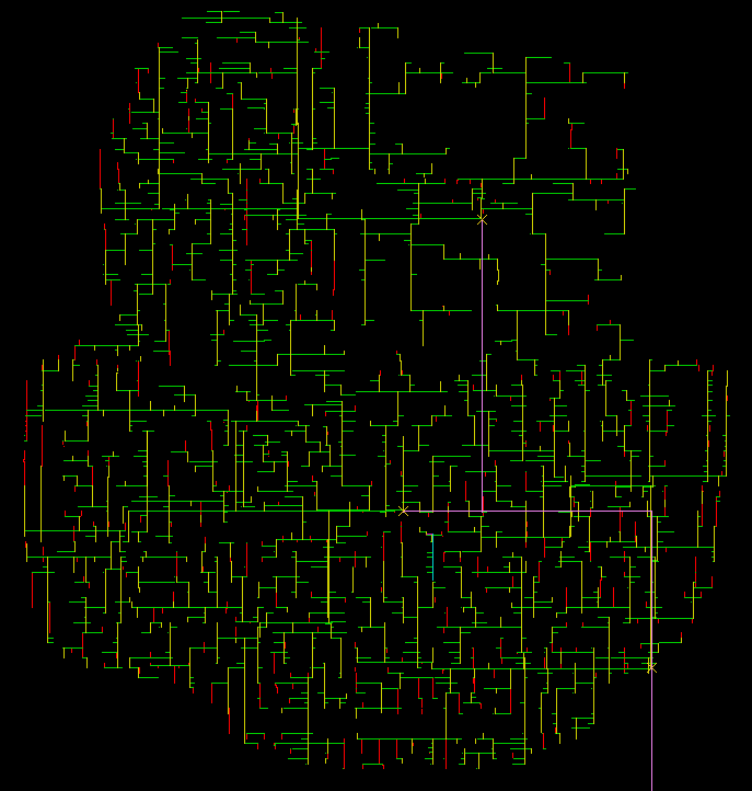
Layout of the AES chip
Layout of the clock tree in the AES chip
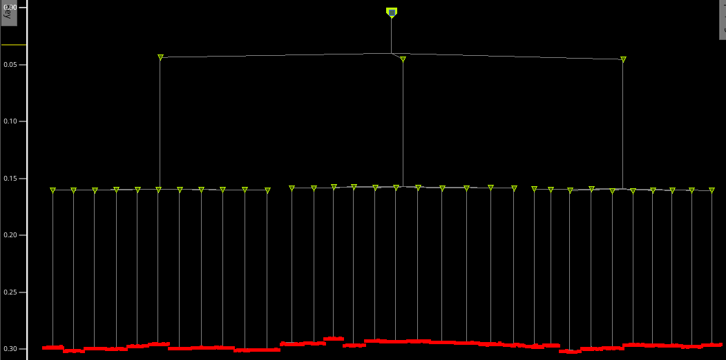
The clock tree is amazingly well balanced showing less than 1ns skew over the entire design