Every year at the conclusion of the codesign class (ECE 4530), I’m organizing a codesign challenge. This is an open-ended design assignment to optimize the performance of an FPGA-based embedded system. The application changes every year, but the performance is characterized by a single metric: the execution time of a reference testbench. The project grade received by the students is proportional to their performance ranking. The fastest design receives the most points, the second-fastest design receives a bit less, and so on. In such an open-ended setting, the difference in design quality delivered by the students is significant (say, orders of magnitude).
This year, we use a DE1-SoC FPGA-board from Terasic. The FPGA chip on this board is a Cyclone V, which includes a dual-core ARMv7 processor that runs at 800MHz, and an FPGA fabric at 50Mhz. The ARMv7 processor runs an embedded Linux kernel.
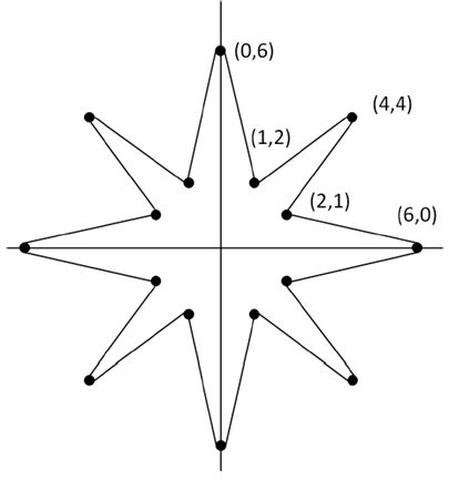
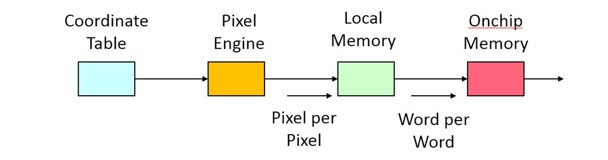
The design problem (online specification , online code) is a pattern generation problem that writes 50 random stars to a bitmapped display constructed in an onchip memory configured in the FPGA. The display holds 1024 by 512 pixels, and each of the 8-pointed starts come in 12 different sizes scaled up from a uniform shape. The star coordinates and sizes are specified in a table, stored in off-chip DDR memory. The algorithm to draw the edges of a star is based on the Bresenham line drawing algorithm, an elegant integer-only algorithm to draw slanted lines on a discrete grid. A star has a high degree of symmetry - we only need to generate two edges of different slopes, and all other edges can be found by mirroring over the X and Y axis. Hence, the design problem is to accelerate the following drawing loop as much as possible.
 for star = 1 to 50
    read xstar, ystar, sizestar from table
       for pixels = 1 to edgepixels on slope 1
          store 8 pixels in FPGA on-chip memory
       for pixels = 1 to edgepixels on slope 2
          store 8 pixels in FPGA on-chip memory
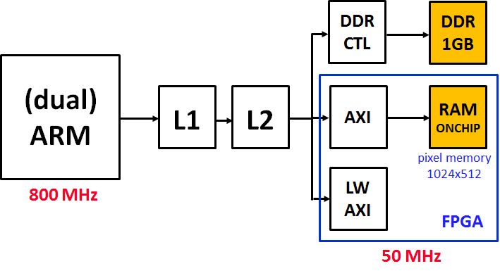
The Cyclone V FPGA has a dual-core ARM processor with two-level cache. The memory hierarchy of the hybrid ARM-with-FPGA includes a 1 GByte off-chip DDR memory, and a set of three AXI bridges to the FPGA memory, each of them attached at the third level of the memory hierarchy.
The resulting structure is one of the extremes. The ARM runs at 800 MHz, 16 times faster than the 50MHz FPGA. So there are 16 ARM cycles for every FPGA cycle. Second, because of the cache hierarchy, the memory read access time to the off-chip 1GByte DDR is about 10 to 20 times shorter than the memory access to the memory configured in the FPGA. When accessing memory in a tight loop, for example, a stack variable access costs 12 cycles, while an FPGA on-chip memory access costs 198 cycles. It’s surprising that the FPGA access is so slow, but most likely this can be explained by the large difference between FPGA clock frequency and ARM clock frequency, and the inability to rely on the cache when writing the FPGA onchip memory.
The slow FPGA memory is a challenge for the star-drawing problem because the memory accesses in the innermost loop are also the most frequent, and the slowest. It takes the reference testbench about 12.9 million ARM clock cycles to finish the drawing of 50 stars. The students of the class had three weeks to solve this problem. We also had two in-class discussion sessions.

The results graph illustrates the logarithm of the speedup as a function of the class population. The speedup is the ratio of the reference testbench cycle count (12.9 million cycles) to the accelerated testbench cycle count. Clearly, there is a significant difference between the fastest design and the slowest design: 328 times speedup versus 1.
The difference of orders-of-magnitude in design quality between the designs from different students does not come as a surprise - I have seen a similar effect every other time I have taught this class (and I wrote this paper on it). A surprise this year, however, was the difference in design strategy between the fastest design and the third-fastest design. The winning design used an all-hardware strategy which migrated the entire problem into the FPGA. Inside of the FPGA, the entire pixel-generation loop can be converted into a set of parallel pixel-plotting engines. Furthermore, the FPGA clock can be increased. The third-fastest design, on the other hand, is an all-software design which pulled the pixel-drawing loop out of the FPGA, and which used multi-threaded programming on the dual-core ARM to accelerate the drawing problem.
In design acceleration problems, there is often a single common strategy that will outperform all other strategies by far, and that will clearly indicate the global optimum. In this case, however, optimizing for an 800MHz ARM and for a 50MHz FPGA both are appealing, and the results of the optimization process are within one order of magnitude from each other. That is both exciting and discomforting: both strategies (software-driven and hardware-driven) are successful, but what if you’re only interested in the very best design?
With the new hard cores integrated with the FPGA in a single package, it looks like hardware software codesign is about to become a lot more interesting, and challenging.