Lecture 11 - The On-chip Bus environment
Introduction
This lecture describes the standard system-on-chip environment, and the opportunities it offers for design customization. Next, it also introduces the on-chip bus as the backbone for SoC architecture, with an application to Platform Designer in Quartus. Finally, we will discuss an end-to-end example of creating a Nios II based system on chip, along with the software setup for that system.
The System-on-Chip
A system-on-chip (SoC) is a programmable architecture that is specialized towards an application domain, a broad group of applications that share common algorithms and a common purpose. Application domains include, for example, mobile communications, vehicle electronics, television and multimedia. In its most basic form, an SoC is a central processor (typically RISC) with additional hardware specialization. You are already familiar with the micro-controller environment, which uses peripherals (Analog-to-Digital converter, Parallel I/O port, Timer, UART, …) to simplify the design of physical interfaces. But the SoC idea is applicable on a much broader basis.
Consider a smart watch. A teardown of such a system demonstrates a high
degree of specialization, at the system (PCB) level, as well as at the
system-on-chip level. At the PCB level, we may find a large number of components
related to smartwatch input/output. This includes a touch display component,
an NFC chip, a capacitive touch sensor, barometer and gyro MEMS, RF TX/RX,
Wifi, Flash memory, SDRAM memory. The central processing component of the
smart watch is a multicore engine as well, with several GPU processors,
one or more CPU, and
a host of interface peripherals (serial and parallel busses) that integrate
the dedication interface chips on the PCB into a single smart watch.
Reports that analyze such complex designs are an interesting read, and
there are plenty of them online.
Consider this Apple Watch 3 teardown and this report on the A9 chip in that watch.
The bottom line, which is important for this class, is to remember the reason for such a degree of specialization in computing, storage and communication. The reason is energy-efficiency. Specialized hardware components are much better at completing tasks faster and with less energy than software. Recall the intrinsic efficiency of silicon (defined in the notes of review lecture 1), which we found to be 30,000 times higher (in GOPS/Watt) compared to the efficiency of an Intel Core i7. It’s clear that the SoC architecture is a cornerstone in a fully connected world of smart devices.
So in this lecture, we will review the basic principles of system-on-chip, that underly the design of these high efficient implementations.
Basic elements in the System-on-Chip
Consider the basic elements in an SoC. An SoC is constructed around a central CPU or system controller, which connects through instruction-cache and data-cache to a high-speed system bus. The high-speed bus is reserved for components that are capable of working at the highest rate. We may typically find instruction- and data-memories, as well as high-speed peripherals such as Direct Memory Access engines. The high-speed bus connects to (one or more) lower-speed bus(es) through a set bridge, which collects low-speed peripherals such as Timers, PIO ports, UARTs and other memory-mapped peripherals.
Figure: System-on-Chip template
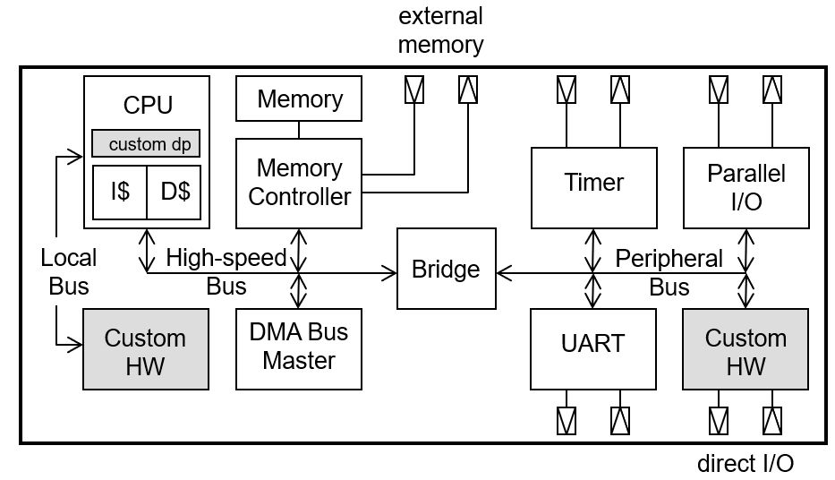
Every component connected to an on-chip bus uses either a master interface or else a slave interface. The communication in such a system is driven by a sequence of bus transactions, and every bus transaction proceeds between a master and a slave. The bus transaction is initiated by a master. A bus write transaction moves data from a master to a slave, and a bus read transaction moves data from a slave to a master. When two masters share the same bus, only one bus transaction can be initiated at a given time, and a every bus transaction must be negotiated using a process called bus arbitration.
A bus master commands an address space and every transaction (read or write) is directed to a specific location in that address space. For example, on a typical 32-bit address bus, a master commands a 4 Gigabyte address space. Every slave on the bus responds to a subset of addresses within the master address space. The slaves on a bus must occupy non-overlapping address ranges.
A transaction on a bus can move as much data as the physical width of the bus allows, and this can be more than one byte. For example, on a 64-bit data bus, up to 8 bytes can be transferred in one bus transaction.
The bus system on an SoC is often segmented, with the different bus segments separated through bus bridges. A bus bridge is a special component that acts like a bus slave on one side, and a bus master on the other side. Bus segmentation helps with two issues. First, it partitions long buses into shorter buses which are easier to implement and which consume less power. Second, it groups components of simular speed and purpose together. A high-speed bus such as the one connected to a CPU is capable of sophisticated, high-speed bus transfers (which we’ll discuss next lecture). But such a bus comes with additional interface design complexity, as every slave connected to the bus must follow the bus protocol. A low-speed bus, such as the one connected to peripherals, only supports simple bus transfers, and is easier to interface.
When designing a system-wide address map, we typically show the map per bus segment or per master. For example, the hypothetical SoC shown above may have a memory map as follows.
| Address From | Adddress To | Segment 1 | Segment 2 |
|---|---|---|---|
| CPU or DMA | Bridge | ||
| 0 | 7FFFFFFF | Memory | |
| 80000000 | 8000FFFF | Bridge | |
| 80000000 | 800000FF | Timer | |
| 80000100 | 800001FF | PIO | |
| 80000200 | 800002FF | UART | |
| 80000300 | 800003FF | Custom HW | |
| 80000400 | 8000FFFF | (unused) | |
| 80010000 | FFFFFFFF | (unused) |
Hardware Customization within the SoC
Within the SoC, there are several opportunities for hardware customization and acceleration. We distinguish three cases, depending on their degree of coupling with the program on the CPU. Loose and tight coupling, in this context, means that the activities in the hardware accelerator are relatively independent (loose coupling), or else tightly synchronized (tight coupling) to the execution of instructions on the CPU.
-
Memory-mapped Coprocessors: A hardware accelerator may be designed as a peripheral, using memory-mapped interfaces. The hardware accelerator operates as an independent unit, that needs to receive or transmit operands from/to the CPU (or DMA).
-
Tightly-coupled Coprocessors: A hardware accelerator may be designed as a specialized peripheral that sits next to the processor on a dedicated, local bus. Such coprocessors are tightly coupled to the execution of instructions on the CPU. The CPU manages the execution of software with fetching of instructions, and the CPU then directs coprocessor instructions to the tightly-coupled coprocessor on the local bus. The CPU has such a local bus by design, and provides instructions specifically intended to operate this local bus.
-
Custom-instruction Coprocessors: A hardware accelerator may be fully integrated into the datapath or execution unit of a CPU. Such a coprocessor is completely integrated within the CPU, and may run as a new instruction on the CPU. This is the most drastic customization, as the designer will now fully customize a CPU, with potential impact on the compiler and assembler tooling for the processor. This type of design has been called ASIP (application-specific instruction-set processor), to indicate that the instruction-set of a processor is adapted towards a given application domain.
From a designer perspective, loose coupling is the easiest design, as it only requires the capability to add a memory-mapped register, to integrate a hardware accelerator. The communication with the hardware proceeds through standard load/store instructions, and the compiler toolflow remains essentially unchanged. The tight coupling tends
From a user perspective, tight coupling tends to simplify the operation of the hardware accelerator, because the loading of operands, control of execution, and retrieval of results, is handled transparently, often as a single coprocessor instruction or custom instruction. In the case of loose coupling, on the other hands, the user has a higher responsibility in the execution of the accelerator hardware - such as loading operands, controlling execution, and retrieving the result.
| Software Interface | Hardware Interface | Portability | |
|---|---|---|---|
| Memory-mapped Coprocessor | load/store instructions | Bus interface | Bus-specific |
| Tightly-coupled Coprocessor | coprocessor instructions | Coprocessor interface | CPU-specific |
| Custom Instruction Coprocessor | custom instructions | full custom | application-specific |
Simple bus transactions
We will now discuss the typical bus transfers in an SoC. Because there are so many different bus standards, we will adopt a generic bus, and highlight various bus transaction concepts. After that, we will give several specific bus standard examples.
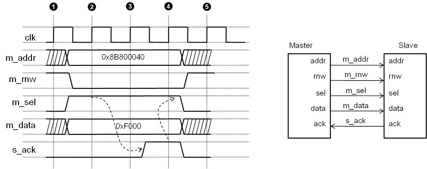
An on-chip bus includes the following signals: an address bus, a data bus, a command bus, and synchornization signals. The address bus carries the master address. The data bus carries data from the master to the slave (m_data) or from the slave to the master (s_data). It is common for an on-chip bus to use directional wires. Tri-state is only used for directional input/output pins, but not for internal wiring. The command bus holds control wires that qualify the bus transaction (such as distinguishin a read from a write). The synchronization signals control the bus timing. All the examples that we will discuss use synchronous, single-clock design.
Table: Signals for simple bus transactions
| type | signal | Purpose |
|---|---|---|
| Synchronization | clk |
Clock signal. All other bus signals are references to the upgoing clock edge. |
| Address | m_addr |
Master Address Bus |
| Data | m_data |
Data bus from master to slave (write operation) |
| Data | s_data |
Data bus from slave to master (read operation) |
| Command | m_rnw |
Read-no-write, indicating the direction of the transaction |
| Command | m_sel |
Master select signal, indicates that this master takes control of the bus. |
| Command | s_ack |
Slave acknowledge signal, indicates transfer completion. |
The common characteristic of a ‘simple’ transfer is that the entire bus transaction
is implemented as a single operation. The master takes control over the bus, broadcasts
an address, and expect one of the slave to acknowledge the address and either accept data (write) or return data (read). The combination of m_sel and s_ack is
reminds of the two-way handshake protocol. And, in fact, is is the same concept.
The advantage of the slave acknowledge signal is that speed of the bus transaction
automatically adjusts to the slower bus component. The extra cycles inserted between
m_sel and s_ack are called wait states. In this particular example, it’s possible
that the slave delays the master indefinitely, simply by not responding. That is clearly
undesirable. To deal with this issue, more advanced bus protocols will define
a bus timeout, an upperbound in the amount of clock cycles that a bus master will wait.
Such bus masters must be capable of aborting a bus transfer.
Figure: Simple Bus Write Transfer
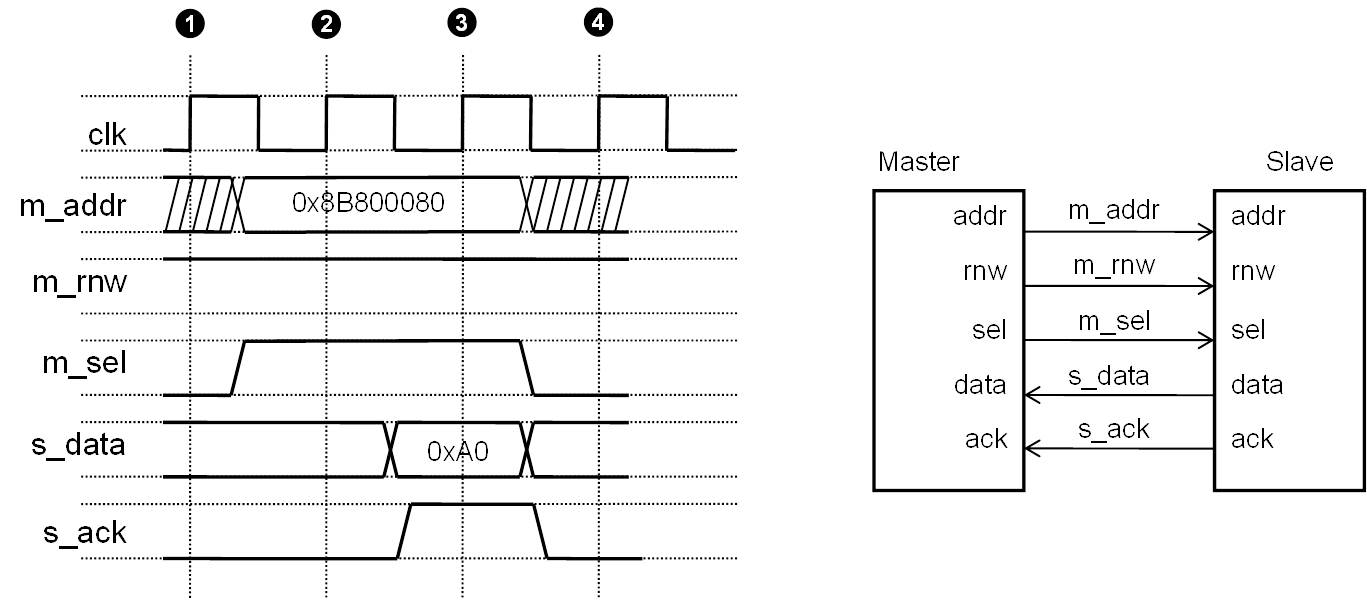
Figure: Simple Bus Read Transfer
Bus Arbitration
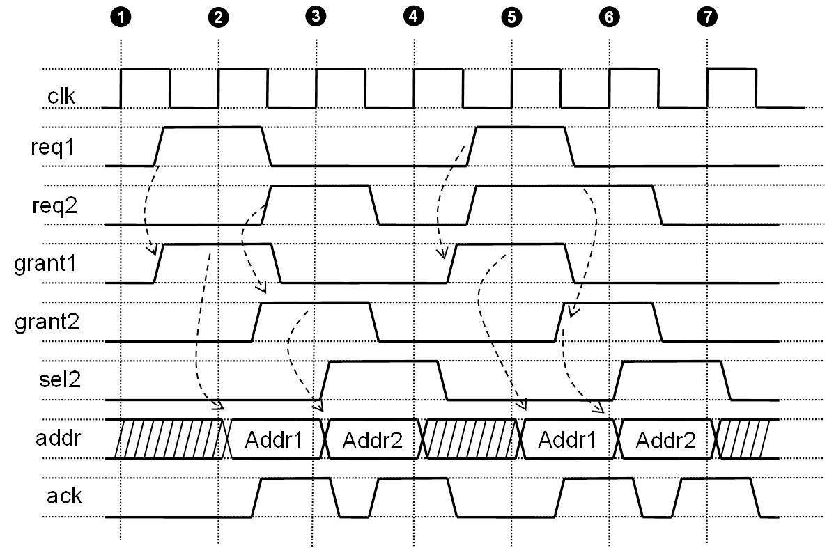
When more then one master is attached to a bus, the access to the bus must be negotiated per bus transaction. That requires the introduction of another compoment, a bus arbiter. The arbiter introduces additional bus handshake signals to help resolve the bus access.
The arbiter uses the requests of all masters and grants the bus to one particular master. This has to follow a bus priority, such as a fixed or rotating priority.
Table: Signals for Bus Arbitration
| type | signal | Purpose |
|---|---|---|
| Command | m_reqi | Master i bus request signal, asking for bus access |
| Command | m_granti | Master i bus grant signal, releasing the bus to master i |
Figure: Bus Arbitration
The Platform Designer Design Flow
Finally, we will discuss an end-to-end example of a Nios based SoC made using Platform Designer. The example is available on github. Unless specified otherwuse, you must do all of the following operations in a Nios II command shell.
git clone https://github.com/vt-ece4530-f19/example-nios-timer
There are two designs nested into each other.
exampleniostimeris the outer design, compiled in Quartus and binding the inner platform to the FPGAplatformniostimeris the inner design, compiled in Platform Designer and generating Verilog code form Quartus.
Synthesizing the hardware
Open the exampleniostimer design in Quartus, and open the Platform Designer in Quartus. Load the platformniostimer design in Platform Designer. You will see an SoC configurarion with five components: a clock source, a NIOS II processor, a 32 Kbyte on-chip memory, a JTAG UART, and a timer. There are also six bus connections: a clock bus, a reset bus, a data master bus, an instruction master bus, an interrupt bus, and a debug reset bus. These six bus connections illustrate different types of interrconnect that are supported in Platform Design; only the data master bus and the instruction master bus correspond to the simple bus system we discussed above. The other connections (clock, reset, interrupt) are of a specialized kind, and will be discussed next lecture.
Figure: Nios Platform
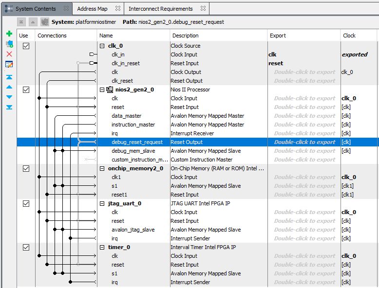
The ‘Address’ tab shows the current address mapping used by the slaves in this system. The addresses of components can be individually selected. It is also possible to assign addresses automatically (System - Assign Base Addresses).
Figure: Nios Address Map

After clicking ‘Generate’, the platform designer creates a verilog view for every component in the system, as well as all the required interconnect. Consider the files generated in platformdesigner.
The ‘bb’ file shows a black-box (top-level) view of the system,
while the ‘inst’ file shows how you would instantiate it in
a top-level verilog. The synthesis subdirectory contains all the generated verilog.
.
├── platformniostimer_bb.v
...
├── platformniostimer_generation.rpt
├── platformniostimer.html
├── platformniostimer_inst.v
├── platformniostimer_inst.vhd
└── synthesis
    ...
    ├── platformniostimer.v
    └── submodules
        ├── altera_avalon_sc_fifo.v
        ...
        └── platformniostimer_timer_0.v
In Quartus, you can now instantiate this platform.
module exampleniostimer(
        input         CLOCK2_50,
        input         CLOCK3_50,
        input         CLOCK4_50,
        input         CLOCK_50,
        input  [3:0]  KEY
);

  wire clk;
  wire rst;

  platformniostimer u0 ( .clk_clk(clk),
                         .reset_reset_n(rst)
                        );

  assign clk = CLOCK_50;
  assign rst = KEY[0];

endmodule
Next, you can synthesize the design, and download the resulting
bitstream to the board. The ‘-d 2’ argument in nios2-configure-sof
selects the second device on the JTAG chain connected to the USB
Blaster. The FPGA on the DE1-SoC board has two independent JTAG
chains: one for the ARM processor (called SOCVHPS), and one for the FPGA (called 5CSE). You can see these two chains listed when you use the jtagconfig command.
quartus_sh --flow compile exampleniostimer
jtagconfig
# output of jtagconfig:
# 1) DE-SoC [USB-1]
#     4BA00477   SOCVHPS
#     02D120DD   5CSE(BA5|MA5)/5CSTFD5D5/..
nios2-configure-sof -d 2 exampleniostimer.sof
Compiling the software
Next, we must implement the software. Compilation of the software goes through two steps. First, we need to generate and compile a board support package, a library with support functions specific for this example. Next, we need to write and compile an application using the board support package.
The Nios2 BSP editor starts from a platform info file, generated by Platform Designer, and extract the required software configuration. We will (1) wire the timestamp_timer to the timer_0 module, (2) select a small C library and (3) select a small JTAG driver. The latter two options ensure that the entire application will fit entirely within the on-chip memory (32Kbyte). Next, we ‘Generate’ the BSP configuration.
nios2-bsp-editor
Figure: Nios NSP Editor
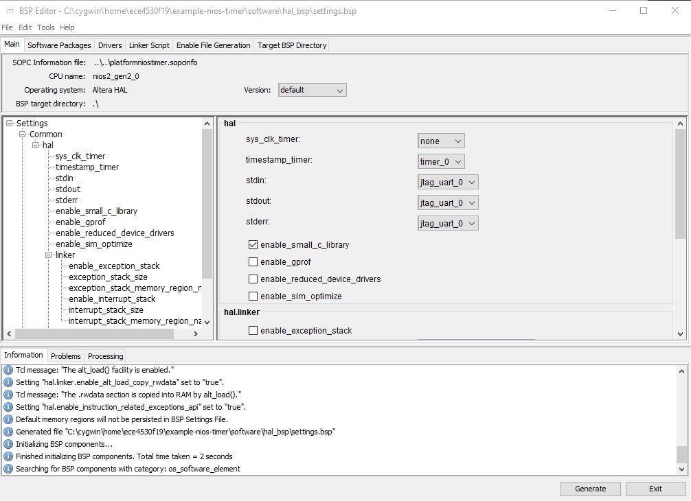
Next, we generate the BSP C source code, and compile it.
nios2-bsp-generate-files --settings=hal_bsp/settings.bsp \
                         --bsp-dir=hal_bsp
cd hal_bsp
make
Note that, again, a large number of files are generated. The most
important of these files is an include file called system.h.
It lists the basic parameters and definitions for each peripheral,
including its base address, as well as specific hardware settings.
Indeed after the hardware design is synthesized, the software has no direct way of determining the precise configuration of the platform. Since each of the peripherals in Platform Designer is highly configurable, the system.h file is used to convey the specific configuration for each peripheral.
Here is an example for the timer module. The system.h indicates this is a 32-bit timer running at 50MHz and attached to an interrupt. The timer is mapped to base address 0x11020. This data complements (the documentation of the timer peripheral)[], which is generic.
/*
 * timer_0 configuration
 *
 */

#define ALT_MODULE_CLASS_timer_0 altera_avalon_timer
#define TIMER_0_ALWAYS_RUN 0
#define TIMER_0_BASE 0x11020
#define TIMER_0_COUNTER_SIZE 32
#define TIMER_0_FIXED_PERIOD 0
#define TIMER_0_FREQ 50000000
#define TIMER_0_IRQ 1
#define TIMER_0_IRQ_INTERRUPT_CONTROLLER_ID 0
#define TIMER_0_LOAD_VALUE 49999
#define TIMER_0_MULT 0.001
#define TIMER_0_NAME "/dev/timer_0"
#define TIMER_0_PERIOD 1
#define TIMER_0_PERIOD_UNITS "ms"
#define TIMER_0_RESET_OUTPUT 0
#define TIMER_0_SNAPSHOT 1
#define TIMER_0_SPAN 32
#define TIMER_0_TICKS_PER_SEC 1000
#define TIMER_0_TIMEOUT_PULSE_OUTPUT 0
#define TIMER_0_TYPE "altera_avalon_timer"
Using the BSP, we next write a small application. The following application computes a modulo-179 operation without making use of integer division, but using only power-of-2 division and power-of-2 modulo. The purpose of the application is to time the execution time for a sample test vector.
Note the inclusion of system.h as well as the inclusion
of sys/alt_timestamp.h.
#include <system.h>
#include <stdio.h>
#include "sys/alt_timestamp.h"

unsigned modk(unsigned x, unsigned k) {
  return (x & ((1 << k) - 1));
}

unsigned divk(unsigned x, unsigned k) {
  return (x >> k);
}

unsigned modulo(unsigned x) {
  unsigned r, q, k, a, m, z;
  m = 0xB3; // 179
  k = 8;
  a = (1 << k) - m;
  r = modk(x, k);
  q = divk(x, k);
  do {
    do {
      r = r + modk(q * a, k);
      q = divk(q * a, k);
    } while (q != 0);
    q = divk(r, k);
    r = modk(r, k);
  } while (q != 0);
  if (r >= m)
    z = r - m;
  else
    z = r;
  return z;
}

int main() {
  volatile unsigned a;
  unsigned i;
  unsigned ticks[10];

  alt_timestamp_start();

  printf("Timer Frequency %u\n", (alt_u32) alt_timestamp_freq());

  printf("Empty call ticks: ");
  for (i=0; i<9; i++) {
    ticks[i] = alt_timestamp();
    ticks[i] = alt_timestamp() - ticks[i];
    printf("%5d ", ticks[i]);
  }
  printf("\n");

  printf("Modulo call ticks: ");
  for (i=0; i<9; i++) {
    ticks[i] = alt_timestamp();
    a = modulo(0x00c0ffee);
    ticks[i] = alt_timestamp() - ticks[i];
    printf("%5d ", ticks[i]);
  }
  printf("\n");

  return 0;
}
To compile the application, we first create a makefile specific for our BSP, and next compile the source code.
nios2-app-generate-makefile     \
             --bsp-dir=hal_bsp  \
             --src-files=main.c \
             --elf-name=main.elf
Finally, we can download and run the application. The JTAG UART peripheral supports the connection of a terminal to the board. Open a second Nios II Command Shell and type
nios2-terminal
In the first Nios II Command Shell, run the application using the following command
nios2-download main.elf --go
In the first terminal, you’ll see the output appear. The application takes 10 time measurements and all of them are identical. There are several reasons for this. The application has no data dependencies, and the architecture does not have a stack. Furthermore, there are no other activites on the platform besides the execution of the software. All of these makes the execution highly regular.
Timer Frequency 50000000
Empty call ticks:   337   337   337   337   337   337   337   337   337
Modulo call ticks: 14350 14350 14350 14350 14350 14350 14350 14350 14350