Lecture 4 - The MSP-430 Hardware Design Flow
- Introduction
- The MSP-430 Hardware
- The msp430de package
- Generation and Instantiation of Memories
- Compiling software for msp430de
- Running the msp430de application
- Conclusions
Introduction
In the big picture of the lecture sequence of the MSP-430, today, we will discuss the hardware.
- Lecture 2: The MSP430 architecture and its implementation in Verilog. Simulation of the MSP430 in Verilog.
- Lecture 3: The embedded software design flow of the MSP-430. The linking process. Compiler opimization.
- Lecture 4: The hardware synthesis flow of the MSP-430 for the DE-1 SoC kit.
- Lecture 5: Performance evaluation using timers.
- Lecture 6: Memory-mapped custom hardware for the MSP-430.
- Lecture 7: Hardware/Software Communication. Using memory-mapped interfaces to call hardware modules from software.
- Lecture 8: Hardware Acceleration. Overhead factors in hardware acceleration.
In lecture 3, we talked about the software design flow for the MSP-430.
- The inputs of the software design flow are (a) a C program and (b) a linker description file.
- The outputs of the software design flow are a binary file, the output of the loader, which represents the contents of the program memory. In addition, the software design flow can produce a listing file, which allows you to understand what the compiler has done.
In this lecture, we start from the outputs of the MSP-430 software design flow, and take those output further into implementation for FPGA.
- The inputs of the hardware design flow are (a) Verilog for the MSP430, including memory cells that can hold the program binary, (b) the software binary, intended to fill up the memory cells, and (c) the binding of the Verilog onto the FPGA pins.
- The output of the hardware design flow is bitstream to program the FPGA on the FPGA board
The MSP-430 Hardware
We are using an open-source version of MSP-430 called openmsp430. The processor is distributed through opencores. The best documentation to learn about how to configure the processor and instantiate it in your design, is to read the openmsp430 documentation.
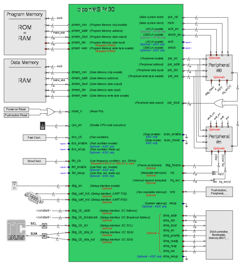
The following Figure, taken from the openmsp430 manual, reflects the top-level interconnect of the design.
-
Only the green block is provided by the openmsp430 design. The core provides additional example peripherals, but the objective is very much that you create your own integration of the core into a bigger system.
-
The system clock input is provided through
dco_clock. The openmsp430 can run at 50MHz on the DE1-SoC board. Furthermore, a system reset can be provided through an external input. -
The core has three bus connections: one for the program memory (
pmem_..), one for the data memory (dmem_..), and one for the peripherals (per_..). The interconnect bus protocol is straightforward.-
In an active bus cycle, the core will assert the bus enable line (
pmem_cen,dmem_cenorper_endepending on the case), and output an address on the address bus (pmem_addr,dmem_addrorper_addr). These addresses are always relative to the start of the program memory, the data memory or the peripheral memory space, and hence they start at 0. -
In a write cycle, the core will also assert the corresponding write-enable (
pmem_wen,dmem_wenorper_wedepending on the case. Thensuffix indicates negative assertion on the logic). -
In a read cycle, the write-enable will not be asserted. During a write-operation, the corresponding data-output (
pmem_din,dmem_dinorper_din) will be asserted. During a read-operation, the corresponding data-input (pmem_dout,dmem_doutandper_dout) will be read. All these bus transactions complete in a single cycle (write) or two cycles (read).
-
-
The list of peripherals connected to the peripheral bus is user-defined. The output databuses going from peripheral back to the core are OR-ed. A peripheral that is inactive will emit a zero-value on the bus, so that an active peripheral on the bus will not be disturbed. Of course, this only works when the peripheral subsystem is correctly configured and no two peripherals act upon the same adress.
-
There are several other subsystems visible on the external interconnect of openmsp430, but we will ignore these (including
slowclk, the debug port, the I2C port, the DMA bus, the scan input, and thenmiinput).
Figure: Top-level interconnect of an openmsp430 system
Configuration of the openmsp430
The openmsp430 design in Homework 1 has the following directory structure.
core
├── bench
│   └── verilog                 verilog testbench for simulation
├── rtl
│   └── verilog                 verilog implementation of the core
│       └── periph              verilog peripherals used by the core
└── sim
    └── rtl_sim                 RTL simulation subdirectoru
        ├── bin
        ├── run                 simulation scripts
        ├── src                 test scripts in assembly
        └── src-c               test scripts in C
            ├── coremark_v1.0
            ├── dhrystone_4mcu
            ├── dhrystone_v2.1
            ├── portops
            └── sandbox
The openmsp430 verilog is stored in the rtl\ directory. The core is highly
configurable through a file openMSP430_defines.v and many parameters
can be set.
- Program Memory Size
- Data Memory Size
- Hardware Multiplier (as a peripheral; the MSP-430 has no multiply instruction)
- Debug Unit (Y/N)
- Version
- Watchdog (Y/N)
- Non maskable interrupt (Y/N)
- Number of interrupts (16/32/64)
- Input port Synchronizers
- Peripheral memory space
- Break on Reset (during a break, control over the CPU is returned to the debug interface)
The top-level in the rtl directory is openMSP430.v. This module contains only
the MSP-430 core, the green block of Figure 1.
When instantiating the openmsp430, you have to set the program memory
size and data memory size to the desired quantity. The memory sizes used in the
configuration file have to correspond to the memory sizes used in the linker
description file of the software flow.
The msp430de package
We next discuss the integration of the MSP-430 in an FPGA. The purpose of this integration is as follows.
-
It supports the openmsp430 core with integrated data memory, program memory and peripherals. Initially, we will include a PIO port, a hardware timer, a UART, and two RAM areas (one serving as data memory and one serving as program memory).
-
It integrates the toplevel onto an FPGA board and provide the proper pin binding for the peripherals present on the board (LEDs, switches, and communication channels).
-
It supports software development for the embedded system covering the openmsp430 with its peripherals. It is able to integrate the resulting binary into the FPGA bitstream.
-
An additional requirement is that the integration must support configuration of the FPGA on the board, using a bitstream that includes hardware and software.
Start by cloning the example repository for this lecture.
git clone https://github.com/vt-ece4530-f19/example-openmsp430de
You will get a repository with MSP-430 hardware and MSP-430 software. The main directories in this package are the following.
example-openmsp430de/
├── hardware               contains hardware designs using MSP-430
│   ├── msp430de0nano      binding of MSP-430 on a DE0-nano board
│   │   ├── msp430         MSP-430 core from opencores
│   │   └── mspconnect     JTAG terminal connection module
│   └── msp430de1soc       binding of MSP-430 on a DE1-SoC board
│       ├── msp430         MSP-430 core from opencores
│       └── mspconnect     JTAG terminal connection module
├── loader                 bitstream downloading and runtime module
└── software               software designs for MSP-430
    ├── demode0nano        example application for a DE0-nano board
    ├── demode1soc         example application for a DE1-SoC board
    └── hal                hardware abstraction layer library
We will focus on the implementation for a DE1-SoC board. The toplevel
of the openMSP430 system (core, peripherals, and memories) is stored in example-openmsp430de/hardware/msp430de1soc/msp430/toplevel.v;
the integration on the FPGA board is stored in example-openmsp430de/hardware/msp430de1soc/msp430de1soc.v.
The FPGA integration
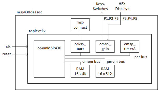
The system-level interconnect of the design integrated on the board is illustrated in the following figure. Three peripherals, a UART, a GPIO port and a timer, are integrated onto the peripheral bus.
The UART and GPIO are connected off-board to a JTAG-UART module (mspconnect) and to keys and hex displays, respectively.
-
The openmsp430 has two UART modules: a user UART and a debug UART. Both UART is accessible through the USB connection of the DE1SoC board.
-
The JTAG-UART module provides UART functionality through the USB cable connected to the DE1SoC kit. This module,
mspconnectis created in QSYS (Platform Designer), a tool which we will discuss in a later lecture. -
The HEX displays make use of a HEX decoder module in hardware. Therefore, one 8-bit PIO port can directly drive two seven-segment displays. The ports are connected such that HEX0 and HEX1 are driven by the lower and upper nibble of P3, HEX2 and HEX3 are driven by P4, and HEX4 and HEX5 are driven by P5.
-
The toplevel also includes a hardware heartbeat counter that blinks a red LED as soon as the bitstream is configured.
Figure: Integration of openmsp430 in DE1SoC
Quartus synthesis
To synthesize the hardware project, open the project msp430de1soc and synthesize it.
You will end up with a bitstream (.sof) file.
The synthesis can be run directly from the command line as well. Open a Nios-II command shell, navigate to the msp430de1soc/hardware directory and use the command:
quartus_sh --flow compile msp430de1soc
The resulting bitstream has a complete hardware design, but the memory cells in this bitstream are still empty. We have to first compile the software, and next integrate the software binary into the bitstream. That is the topic of the next part.
Generation and Instantiation of Memories
Perhaps the most complex operation for the implementation of this system on FPGA involves the configuration, generation, and instantiation of the data and program memory. In brief, the steps involve the following.
-
Select the appropriate memory size for the memory in the
openmsp430_defines.vconfiguration file -
Instantiate the memory correctly in the system interconnect
-
Generate the memory as an IP module in the Quartus FPGA design environment
-
Adjust the linker description file to reflect the proper memory layout
We will investigate each of these steps for the case of our design, which will use a 1KB program memory and an 8KB data memory. These memories will be configured as a 512 word program memory and a 4KB word data memory, respectively.
Select the appropriate memory size
The first step, configuration of the sizes, is done by uncommenting the appropriate line in openmsp430_defines.v.
// Program Memory Size:
//                     Uncomment the required memory size
//-------------------------------------------------------
//`define PMEM_SIZE_CUSTOM
//`define PMEM_SIZE_59_KB
//`define PMEM_SIZE_55_KB
//`define PMEM_SIZE_54_KB
//`define PMEM_SIZE_51_KB
//`define PMEM_SIZE_48_KB
//`define PMEM_SIZE_41_KB
//`define PMEM_SIZE_32_KB
//`define PMEM_SIZE_24_KB
//`define PMEM_SIZE_16_KB
//`define PMEM_SIZE_12_KB
//`define PMEM_SIZE_8_KB
//`define PMEM_SIZE_4_KB
//`define PMEM_SIZE_2_KB
`define PMEM_SIZE_1_KB


// Data Memory Size:
//                     Uncomment the required memory size
//-------------------------------------------------------
//`define DMEM_SIZE_CUSTOM
//`define DMEM_SIZE_32_KB
//`define DMEM_SIZE_24_KB
//`define DMEM_SIZE_16_KB
//`define DMEM_SIZE_10_KB
`define DMEM_SIZE_8_KB
//`define DMEM_SIZE_5_KB
//`define DMEM_SIZE_4_KB
//`define DMEM_SIZE_2p5_KB
//`define DMEM_SIZE_2_KB
//`define DMEM_SIZE_1_KB
//`define DMEM_SIZE_512_B
//`define DMEM_SIZE_256_B
//`define DMEM_SIZE_128_B
Instantiate memory in the system interconnect
Next, we instantiate each memory in the toplevel interconnect for the openMSP430. Here is the data memory. The interconnect uses a 12-bit address, which reaches each of the 4096 RAM locations. The data memory bus, like all on-chip memory busses, is non-multiplexed. There is a separate connection for data from MSP430 to the memory (dmem_din) and for data from memory to MSP430 (dmem_dout). The reason is that on-chip wires are relatively chip compared to the overhead of a multiplexed (bidirectional) bus. In addition, point-to-point connections are easier to verify. The RAM will transfer 16 bits per clock cycle from the core to the RAM, or in the other direction.
   ram16x4096 ram (
                   .address (dmem_addr[11:0]),
                   .clken   (~dmem_cen),
                   .clock   (clk_sys),
                   .data    (dmem_din[15:0]),
                   .q       (dmem_dout[15:0]),
                   .wren    ( ~(&dmem_wen[1:0]) ),
                   .byteena ( ~dmem_wen[1:0] )
                   );
Two control signals, wren and byteena, define the specific operation of the ram. wren is a single-bit write-enable pin that marks the current cycle as a write cycle. byteena is a two-bit signal that marks what bytes are involved in the write transfer. Both of these signals are extracted from a two-bit MSP-430 signal dmem_wen. Recall
that the MSP-430 memory address space is byte addressable, but that the data bus is a 16-bit data bus. Read operations from memory will always transfer 16 bits, regardless of how many the specific MSP-430 instruction will use. Write operations to memory will transfer 16 bits, the low-8 bits of 16 bits, or the high-8 bits of 16 bits, depending on the write-operation performed by the MSP-430. Hence, we can map the memory space operations of the MSP-430 to RAM address and control signals as follows.
| MSP-430 Operation | MSP-430 Address | dmem_addr |
dmem_wen |
wren |
byteena |
|---|---|---|---|---|---|
| read word | 0x0100 | 0x080 | 0b11 | 1 | 00 |
| read byte | 0x0100 | 0x080 | 0b11 | 1 | 00 |
| read byte | 0x0101 | 0x080 | 0b11 | 1 | 00 |
| write word | 0x0100 | 0x080 | 0b00 | 0 | 11 |
| write byte | 0x0100 | 0x080 | 0b10 | 0 | 01 |
| write byte | 0x0101 | 0x080 | 0b01 | 0 | 10 |
The program memory is configured similarly. The physical design of the program memory uses a large memory size, and Verilog macros are used to select a portion of the available memory space. In this case, we have a 512-word logical program memory, which requires 9 address bits. The physical design uses a 27KB memory, which requires 15 address bits.
   ram16x27648 rom (
`ifdef PMEM_SIZE_1_KB
                    .address ({6'b111111, pmem_addr[8:0]}),
`endif
`ifdef PMEM_SIZE_54_KB
                    .address (pmem_addr[14:0]),
`endif
                    .clken   (~pmem_cen),
                    .clock   (clk_sys),
                    .data    (pmem_din[15:0]),
                    .q       (pmem_dout[15:0]),
                    .wren    (~(&pmem_wen[1:0]) ),
                    .byteena (~pmem_wen[1:0])
                    );
Generate a memory IP module in Quartus
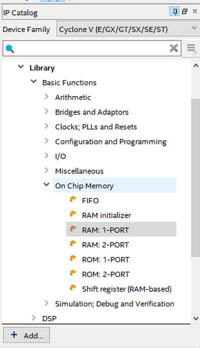
With the memory sizes determined, we now will use Quartus to generate the data memory and program memory IP modules. Both the program and data memory can be created as 1-port RAM modules. In Quartus, use the IP Catalog to find and instantiate these modules.
Figure: Quartus IP Catalog to create a 1-port RAM
Unlike ASIC RAM memories, FPGA RAM memories are synchronous, and require one cycle for access.
Figure: Quartus RAM IP Generation
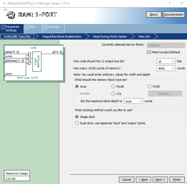
The result of the IP generation process is a black-box .qip (Quartus IP) file
that can be added to a project.
Adjust the linker description file to reflect the proper memory layout
Finally, the linker description file used for software compilation must be adjusted to reflect the selected memory sizes for the program and data memory. This is done by making changes to the MEMORY block. As an example, here is the definition for a memory map with 24KB of program memory and 16 KB of data memory:
MEMORY {
  SFR              : ORIGIN = 0x0000, LENGTH = 0x0010
  RAM (wx)         : ORIGIN = 0x0200, LENGTH = 0x4000
  ROM (rx)         : ORIGIN = 0xA000, LENGTH = 0x6000-0x20
}
Assignment: Complete the memory section in the linker description file for the system we’re building here (8KB data, 1KB program)
MEMORY {
  SFR              : ORIGIN = 0x0000, LENGTH = 0x0010
  RAM    (rwx)     : ORIGIN =       , LENGTH =
  ROM    (rx)      : ORIGIN =       , LENGTH =
}
Compiling software for msp430de
IMPORTANT: Before you compile software with MSP430DE, make sure to install the package
msp430-gcc-support-files-1.207.zipin your compiler directories. These files are needed in addition to the compiler itself, which ismsp430-gcc-8.2.0.52_win64.zip. Refer to the software installation guidelines, which have been updated 9/4/2019.
The software design flow used for applications on the FPGA board uses the same concepts as the software design flow discussed previously. Applications on C code are compiled, linked and loaded into a memory image for the MSP-430 program memory. To isolate the development of application software from the development of hardware, we make use of a hardware abstraction library (HAL). The hardware abstraction library talks directly to hardware peripherals, and provides an application programming interface (API) to work with these peripherals.
Hardware Abstraction Library
Let’s consider a few API functions used by the hardware abstraction library. A few of them are related to the use of the PIO ports, and their integration to the HEX displays.
Here’s (part of) the file omsp_de1soc.c.
The seven-segment decoding decoding for the hex displays is done in hardware. Therefore, only three trivial functions are needed to drive the displays.
void de1soc_ledr(int v) {
  P1OUT = v;
}

void de1soc_hexlo(int v) {
  P3OUT = v;
  P4OUT = (v >> 8);
}

void de1soc_hexhi(int v) {
  P5OUT = v;
}
The HAL functionality for the user UART is slightly more complicated, as it requires proper configuration of the UART peripheral of the MSP-430. The initialization function uartinit sets the baudrate selection, and enables UART receive interrupts. The send function putchar is a blocking-send that loads the transmitter buffer register with a character as soon as it is empty. The receive function INT_uart_rx is an interrupt-service routine that stores the most recently received character in a global variable, rxdata. The function is not sophisticated at all, and does not provide character buffering.
// BAUD = (mclk_freq/baudrate)-1 => 115200  @50Mhz
#define BAUD 433

void uartinit() {
  UART_BAUD = BAUD;          // Init UART
  UART_CTL  = UART_EN | UART_IEN_RX;
}

int putchar (int txdata) {
  while (UART_STAT & UART_TX_FULL);
  UART_TXD = txdata;
  return 0;
}

char rxdata;

wakeup interrupt (UART_RX_VECTOR) INT_uart_rx(void) {
  rxdata = UART_RXD;
  UART_STAT = UART_RX_PND;
}
The compilation of such a hardware abstraction library results in a collection of object files that are combined in an archival library format. Perform the following steps to compile the HAL. If you see an error message during compilation, inspect it. Most likely it is related to a setting (path or tool name) in Makefile.
$ cd msp430de/software/hal
$ make compile
/cygdrive/c/ti/msp430-gcc/bin/msp430-elf-gcc -Wall -Os -mmcu=msp430c1111 -Ic:/ti/msp430-gcc/include -c -o omsp_de0nano.o omsp_de0nano.c
/cygdrive/c/ti/msp430-gcc/bin/msp430-elf-gcc -Wall -Os -mmcu=msp430c1111 -Ic:/ti/msp430-gcc/include  -c -o omsp_de1soc.o omsp_de1soc.c
/cygdrive/c/ti/msp430-gcc/bin/msp430-elf-gcc -Wall -Os -mmcu=msp430c1111 -Ic:/ti/msp430-gcc/include -c -o omsp_delay.o omsp_delay.c
/cygdrive/c/ti/msp430-gcc/bin/msp430-elf-gcc -Wall -Os -mmcu=msp430c1111 -Ic:/ti/msp430-gcc/include  -c -o omsp_uart.o omsp_uart.c
/cygdrive/c/ti/msp430-gcc/bin/msp430-elf-ar r libomsp_de.a omsp_de0nano.o omsp_de1soc.o omsp_delay.o omsp_uart.o
C:\ti\msp430-gcc\bin\msp430-elf-ar.exe: creating libomsp_de.a
/cygdrive/c/ti/msp430-gcc/bin/msp430-elf-size *.o
   text    data     bss     dec     hex filename
     42       0       0      42      2a omsp_de0nano.o
     64       0       0      64      40 omsp_de1soc.o
     40       0       0      40      28 omsp_delay.o
     54       0       0      54      36 omsp_uart.o
Example Application
Here is the complete application for msp430de. It makes use of the HAL functions we just discussed. The application is a busy while loop that maintains two counters, c and k. At each iteration, it sends the counter value to the UART as a hex string. It also displays the counter value on the HEX displays, and flashes the red leds in a shifting order.
#include "omsp_de1soc.h"

char c16[]={'0','1','2','3','4','5','6','7','8','9','A','B','C','D','E','F'};

void myprintf(char *c) {
  while (*c)
    putchar(*c++);
}

int main(void) {
  register unsigned char k;
  int c = 0;

  de1soc_init();

  while (1) {
    k = 1;
    do {
      putchar(c16[((c>>12) & 0xF)]);
      putchar(c16[((c>>8 ) & 0xF)]);
      putchar(c16[((c>>4 ) & 0xF)]);
      putchar(c16[((c    ) & 0xF)]);
      putchar('\n');
      de1soc_ledr(k);
      de1soc_hexlo(c);
      de1soc_hexhi(c);
      long_delay(100);
      k <<= 1;
      c++;
    } while (k);
  }

  myprintf("exit program\n");

  dint();
  LPM0;

  return 0;
}
We compile the program with make. The size of the executable increases from compiling the main function by itself (182 bytes), to the overall executable (548 bytes).
$ make compile
/cygdrive/c/ti/msp430-gcc/bin/msp430-elf-gcc  -I../hal -Wall -Os -mmcu=msp430c1111 -Ic:/ti/msp430-gcc/include  -c main.c -o main.o
/cygdrive/c/ti/msp430-gcc/bin/msp430-elf-size main.o
   text    data     bss     dec     hex filename
    182      16       0     198      c6 main.o
/cygdrive/c/ti/msp430-gcc/bin/msp430-elf-gcc  -mmcu=msp430c1111 -T linker.x  -L../hal  main.o -lomsp_de -o led.elf
/cygdrive/c/ti/msp430-gcc/bin/msp430-elf-size led.elf
   text    data     bss     dec     hex filename
    548      20       6     574     23e led.elf
/cygdrive/c/ti/msp430-gcc/bin/msp430-elf-objdump -dSt led.elf >led.lst
/cygdrive/c/ti/msp430-gcc/bin/msp430-elf-objcopy -I elf32-msp430 -O binary led.elf led.bin
The second command shows how an object file is linked with the HAL library. The -L flag sets the library path, and the -l flag sets the library name. For example,
-L../hal -lomsp_de expands to the library ../hal/libomsp_de.a. The lib prefix and .a suffix are implicit and always added; they do not have to be added to the -l flag.
/cygdrive/c/ti/msp430-gcc/bin/msp430-elf-gcc -mmcu=msp430c1111 -T linker.x -L../hal main.o -lomsp_de -o led.elf
The final output of the compilation step consists of a listing file, and a binary file (bin). The binary file is an alternative format to the format we discussed last lecture, but has the same purpose.
/cygdrive/c/ti/msp430-gcc/bin/msp430-elf-objdump -dSt led.elf >led.lst
/cygdrive/c/ti/msp430-gcc/bin/msp430-elf-objcopy -I elf32-msp430 -O binary led.elf led.bin
To find out what functions have been compiled into main, and into led.elf, we can use the msp430-elf-nm utility as follows. The three column format displays known and unknown references in this object file. For example, c16 is defined data symbol (D) while de1soc_hexhi is an undefined (U) function referenced in this object file.
$ msp430-elf-nm.exe main.o
         U __crt0_movedata
         U __mspabi_func_epilog_2
         U __mspabi_srai
         U __mspabi_srli
00000000 D c16
         U de1soc_hexhi
         U de1soc_hexlo
         U de1soc_init
         U de1soc_ledr
         U long_delay
0000001c T main
00000000 T myprintf
         U putchar
The msp430-elf-nm output from led.elf is much longer. The following listing has been shortened to keep only T text, D data , and B bss references. We can spot three types of functions: functions from the original object file(s) main.o, HAL library functions, and C library functions. The C library functions can be refined further into traditional library functions (such as memmove), C runtime functions (such as __crt0_start), and ABI functions (such as __mspabi_srai).
$ msp430-elf-nm.exe led.elf
00000210 B __bssstart
0000fc2a T __crt0_call_init_then_main
0000fc08 T __crt0_init_bss
0000fc16 T __crt0_movedata
0000fc04 T __crt0_start
00000200 D __datastart
00000216 B __heap_end__
00000212 B __heap_start__
00000216 B __HeapLimit
0000fe1e T __msp430_fini
0000fe24 T __msp430_fini_end
0000fe14 T __msp430_init
0000fe1e T __msp430_init_end
0000fd94 T __mspabi_func_epilog_1
0000fd92 T __mspabi_func_epilog_2
0000fd90 T __mspabi_func_epilog_3
0000fd8e T __mspabi_func_epilog_4
0000fd8c T __mspabi_func_epilog_5
0000fd8a T __mspabi_func_epilog_6
0000fd88 T __mspabi_func_epilog_7
0000fd9c T __mspabi_srai
0000fda8 T __mspabi_srli
00000210 D _edata
00000212 B _end
00000200 D c16
0000fd26 T de1soc_hexhi
0000fd16 T de1soc_hexlo
0000fcec T de1soc_init
0000fd10 T de1soc_ledr
00000212 B end
0000fd74 T INT_uart_rx
0000fd32 T long_delay
0000fc52 T main
0000fdae T memmove
0000fdfc T memset
0000fc36 T myprintf
0000fd62 T putchar
00000210 B rxdata
0000fd2c T short_delay
0000fd54 T uartinit
Running the msp430de application
We are now read to run the application on the DE1SoC board. You have to make the following setup to complete the experiment.
- If you did not already do so, download the git repository. In a cygwin shell, use the following command.
$ git clone https://github.com/vt-ece4530-f19/example-openmsp430de
$ cd example-openmsp430de
- Compile the FPGA hardware into a bitstream (.sof). In a Nios-II command shell, use the following command.
$ cd  example-openmsp430de/hardware/msp430de1soc
$ quartus_sh --flow compile msp430de1soc
- Compile the software. In the cygwin shell, use the following command.
$ cd software
$ make compile
- Power up the DE1-SoC board (these boards will be distributed next week). Connect the USB blaster port to your PC. Check if the port correctly connects by using the following command in the Nios-II command shell. The command will reply with the board that is recognized by the PC. If nothing appears, verify your USB connection.
$ jtagconfig
1) DE-SoC [USB-1]
  4BA00477   SOCVHPS
  02D120DD   5CSE(BA5|MA5)/5CSTFD5D5/..
- Run the application. In the Nios-II command shell, navigate to the loader subdirectory and use the following command. This script will download the bitstream, connect to the JTAGUART, and then use the MSP430 debug port to download the binary image. The partial output of the tool is shown next.
$ cd ../loader
$   system-console -cli \
      --script connect.tcl \
      -bin ../software/demode1soc/led.bin  \
      -sof ../hardware/msp430de1soc/msp430de1soc.sof
--------------------------------------------------------------------------------
 Version 18.1 625
 Copyright (C) 2018 Intel Corporation. All rights reserved.
 Your use of Intel Corporation's design tools, logic functions
 and other software and tools, and its AMPP partner logic
 functions, and any output files from any of the foregoing
 (including device programming or simulation files), and any
 associated documentation or information is expressly subject
 to the terms and conditions of the Intel Program License
 Subscription Agreement, the Intel Quartus Prime License Agreement,
 the Intel MegaCore Function License Agreement, or other
 applicable license agreement, including, without limitation,
 that your use is for the sole purpose of programming logic
 devices manufactured by Intel and sold by Intel or its
 authorized distributors.  Please refer to the applicable
 agreement for further details.
--------------------------------------------------------------------------------
% INFO: Configuring SOF ../hardware/msp430de1soc/msp430de1soc.sof
Info: *******************************************************************
Info: Running Quartus Prime Programmer
Info: Command: quartus_pgm --no_banner --mode=jtag --cable="DE-SoC on localhost [USB-1]" --operation=p;C:\cygwin\home\ece4530f19\example-openmsp430de\loader\..\hardware\msp430de1soc\msp430de1soc.sof@2
Info (213045): Using programming cable "DE-SoC [USB-1]"
Info (213011): Using programming file C:/cygwin/home/ece4530f19/example-openmsp430de/loader/../hardware/msp430de1soc/msp430de1soc.sof with checksum 0x0149D5F4 for device 5CSEMA5F31@2
Info (209060): Started Programmer operation at Thu Sep 05 11:09:30 2019
Info (209016): Configuring device index 2
Info (209017): Device 2 contains JTAG ID code 0x02D120DD
Info (209007): Configuration succeeded -- 1 device(s) configured
Info (209011): Successfully performed operation(s)
Info (209061): Ended Programmer operation at Thu Sep 05 11:09:32 2019
Info: Quartus Prime Programmer was successful. 0 errors, 1 warning
    Info: Peak virtual memory: 4445 megabytes
    Info: Processing ended: Thu Sep 05 11:09:32 2019
    Info: Elapsed time: 00:00:04
    Info: Total CPU time (on all processors): 00:00:02
INFO: Configuration completed
INFO: Opening JTAG master
MSP430 version=3 mpy=1 dmem=8192 pmem=1024
INFO: Downloading MSP430 binary ../software/demode1soc/led.bin
Downloading ../software/demode1soc/led.bin ..
................*
Download complete. Transfer time: 719243 microseconds per iteration
INFO: Download completed
INFO: Opened socket on port 19800
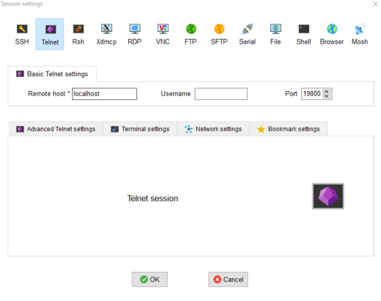
- Finally, you can connect a terminal to the running application. Open MobaXterm, and open a telnet session to localhost port 19800. You can leave the username blank. When the telnet session connects, you will see characters send from the msp430 user UART.
Figure: Moba Xterm telnet configuration to connect to DE1-SoC running msp430de
- To terminate the application, press ctrl-c in the nios-II command shell window
where you started the
connect.tclscript. The prompt will return, but the application will continue to run on the DE1-SoC board. If you opened a telnet connection to the board, you will notice that the telnet connection dies as soon as theconnect.tclscript dies.
Conclusions
In this lecture we’ve covered quite a bit of ground. We discussed the following elements.
- The architecture of the openmsp430 package, and its integration on an FPGA board.
- The configuration of an MSP-430 core, with the selection of memory sizes.
- The generation and instantiation of memory modules in the FPGA environment.
- The concept of Hardware Abstraction Library
- The software design flow for MSP430 when we are using a HAL
- All the steps needed to combine a bitstream and software binary for msp430de on a DE1-SoC board
Next week, we will distribute the DE1-SoC kits, and do a homework around this design concept.